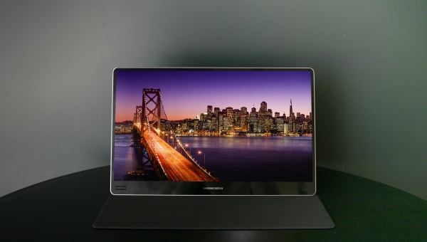
FMM use reaching limit in increasing OLED panel size

Image: Samsung Display
There was increasing interest within Samsung Display in technologies that can be applied to manufacture OLED panels without the use of fine metal masks (FMM), TheElec has learned.
This interest was sparked after the Society of Information Display conference held in May this year where new production technologies of OLED panels were showcased, sources said.
FMM are commodities used to deposit the red, green, and blue OLED subpixels closely together during OLED panel production.
All OLED panels used in smartphones and smartwatches currently commercialized are made with FMM during production, and Dai Nippon Printing is the world’s largest supplier of the commodity.
FMM are made into sticks and multiple units of them are soldered into large frames so that the middle of them doesn’t sag when in use. They sag because they are incredibly thin. The sticks must also be narrow so that they can be pulled tight when put into the frame.
Because of these difficulties, there is increasing concern that FMM won’t be applicable for OLED panels exceeding 15-inch to 17-inch in size made for application in portable devices. Bigger panels require large FMMs.
Currently, FMM production yields are only around 30% for the production of 6-inch OLED panels, and larger panels will result in even lower yields.
Considerably larger OLED panels around 30-inch for automobiles don’t face this problem and the panels themselves are narrow and long, unlike TV panels.
For OLED monitor and TV panels, Samsung Display and LG Display currently use open metal masks rather than FMM as they don’t need to be as fine as those for smaller panels.
Therefore the area of between 17-inch and 30-inch for OLED panels is a new area for display panel makers and a considerable headache for them to decide what production technologies to use.
OLED panel production without the use of FMM has been talked about for the past five years but JDI’s unveiling of its eLEAP technology last year has increased interest.
This year, Japan’s Semiconductor Energy Laboratory (SEL) also filed patents related to OLED panel production without the use of FMM.
During SID in May, JDI and SEL showcased their technologies while Visionox also announced their own version called ViP.
Sources said SEL employees visited Samsung Display and explained their technologies.
Another source who attended SID said, unlike others, SEL’s prototype shown during the conference showed no defect, SEL’s encapsulation process was in a different order than the others, they said.
A separate source said SEL did the encapsulation after the lithography process, while JDI and Visionox did the encapsulation process first.
Conventionally, encapsulation is done first to avoid exposure to water and oxygen as lithography may involve wet etching.
But SEL’s used a special material to avoid the OLED pixels from being exposed to water and oxygen, they said.
Sources within Samsung Display said the company is showing interest in such technologies but is also concerned about the obstacles they face.
One of them is securing exclusive rights over them which will be difficult. Samsung Display prefers to have total control over the market when entering new markets by securing all related patents and technologies to prevent competitors from entering.


