OnChip’s advanced wafer fabrication facility offers backside metallization (BSM) of thin films for various applications such as military, medical, and instrumentation. Back-metal is required on a wide range of Semiconductors devices to form a solderable die attach metal stack to ensure good electrical contact to the chip (ohmic contact) or proper bonding of the chips to their mounting cases. Power devices such as High Brightness Light Emitting Diodes (HB LED) require backside metal for an improved and reliable thermal conductivity. These metal layers are deposited using RF or DC sputtering and electron beam evaporation.
 |
|
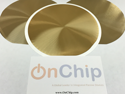
OnChip's wafer fabrication facility offers backside metallization (BSM) of thin films for various applications such as military, medical, and instrumentation.(OnChip/LEDinside) |
In backside metallization of discrete devices, the typical layer stack consists of three to four metal layers. The most common metal stack consists of sputter deposited Titanium (500 Angstroms) followed by Nickel (3,000 Angstroms), and finally a flash of Gold (200 Angstroms). Below is a list of all metals offered by OnChip:
Layers for providing good Ohmic Contact: Gold, Aluminum and Titanium
Barrier and superior Adhesion Layer: Copper, Chromium, Palladium and Titanium
Solder Layers: Nickel, Gold and Silver
OnChip’s systems deposit ultra-clean metal and dielectric films in a class-100 cleanroom. Generally, an in-situ RF etch is performed prior to sequential deposition of multilayers to insure good film adhesion and ohmic contact to underlying conductive layers or to the bare silicon. All sputter films are currently available on silicon wafer sizes up to 150mm (6”) in diameter. Larger wafer sizes may be considered on a case-by-case basis.
Availability and Pricing
The OnChip BSM processing is available immediately worldwide and the Lot Charge ranges from $750.00 to $1,450.00 (depending on metal stack, thickness of layers, wafer diameter, etc.). Typical lot size is 11 for 100mm (4”) wafers, 9 for 125mm (5”) wafers, and 7 for 150mm (6”) wafers. Typical lead times are 2 weeks ARO. The wafers are handled at OnChip Devices' Santa Clara facility and are produced to the highest quality standards.


