Sumitomo Chemical will participate in SPIE Photonics West 2025, the world’s largest optics and photonics conference and exhibition, to be held in San Francisco, California, the United States, from Tuesday, January 28 to Thursday, January 30, 2025. This conference, organized by the International Society for Optics and Photonics (SPIE), the leading society in this field, showcases a wide range of the latest optical and photonic technologies and applications, including optical communications, lasers, and optoelectronic devices.
Sumitomo Chemical offers compound semiconductor products that are garnering attention as next-generation materials. For optical and photonic applications, the Company is developing gallium nitride (GaN) substrates meeting the demand for higher laser output power in particular. At SPIE Photonics West 2025, the Company will exhibit GaN substrates for blue laser diodes and gallium arsenide (GaAs) epitaxial wafers used in vertical cavity surface emitting laser (VCSEL) applications. In addition, Hajime Fujikura, Fellow, ICT & Mobility Solutions Research Laboratory, Sumitomo Chemical, will present an invited talk at the conference on Monday, January 27, the day before the exhibition starts. You are invited to attend his invited talk and visit the Company's exhibition booth.
1. Overview of the Exhibition
SPIE Photonics West 2025
Date: Tuesday, January 28 to Thursday, January 30, 2025
Venue: The Moscone Center, San Francisco, California, the United States
Website: https://spie.org/conferences-and-exhibitions/photonics-west/photonics-west-exhibition
Sumitomo Chemical’s booth number: 4110
(For more information, please see Sumitomo Chemical Co., Ltd. : SPIE Photonics West 2025 Exhibition.)
2. Sumitomo Chemical’s Exhibitions
Compound semiconductor products:
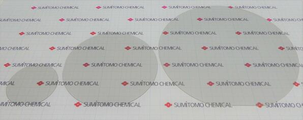
- GaN substrates
Sumitomo Chemical provides high-quality GaN substrates used in optical and electronic devices. The Company is developing higher-quality GaN substrates that will improve the performance of highly efficient laser metal processing machines, mercury-free laser light source projectors, and other optical and electronic devices that contribute to reducing environmental impact.
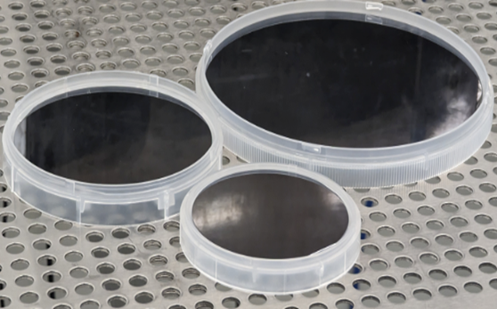
- GaAs epitaxial wafers for use in VCSEL diodes
VCSELs are expected to be used in a broad range of applications, including facial recognition devices and light detection and ranging (LiDAR) devices. Sumitomo Chemical produces GaAs epitaxial wafers for VCSELs tailored to meet customer needs.
3. Sumitomo Chemical’s Invited Talk
Title: Recent progress in HVPE-based GaN substrate fabrication
Presenter: Hajime Fujikura (Fellow, ICT & Mobility Solutions Research Laboratory, Sumitomo Chemical Co., Ltd.)
Date: Monday, January 27, 10:45 a.m. to 11:15 a.m. PST
Abstract of the Presentation: For more information, please see
Recent progress in HVPE-based GaN substrate fabrication | SPIE Photonics West
TrendForce 2025 Infrared Sensing Application Market and Branding Strategies
Release: 01 January 2025
Format: PDF / EXCEL
Language: Traditional Chinese / English
Page: 196
|
If you would like to know more details , please contact:
|


