 2014-06-13
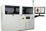
The MicroSense UltraMap C200A is an automated LED Sapphire Wafer Measurement system based on MicroSense's proprietary two sided capacitive sensing technology. The system measures critical substrate parameters including Thickness, TTV, Bow, Warp and Local Thickness Variation (LTV) with high throughput. The UltraMap C200 is designed for sapphire wafer manufacturers and LED chip makers who require better wafer geometry inspection with higher measurement repeatability, compared to traditional optical metrology systems.
Continue reading →
 2014-06-13


