 2015-03-13
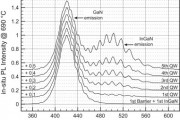
In a collaboration between LayTec and Prof. Dirk Rueter´s group at University of Applied Sciences Ruhr West a breakthrough has been achieved regarding the real-time monitoring of InGaN/GaN quantum well emission wavelength during MOCVD growth. It is well known that room temperature wafer based photoluminescence (PL) measurements provide an excellent forecast of the emission wavelength and emission intensity of the later LED devices. Recently, a prototype in-situ PL system worked simulatnneously with a LayTec Pyro 400 in a commercial multi-wafer MOCVD reactor. The related paper [2] was rocketed immediately to the status of “most downloaded Journal of Crystal Growth articles” from Science Direct. This work is supported under grant KF3242801NT3 by BMWi (German Federal Government).
Continue reading →
 2015-03-13


