 2015-03-13
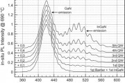
In a collaboration between LayTec and Prof. Dirk Rueter´s group at University of Applied Sciences Ruhr West a breakthrough has been achieved regarding the real-time monitoring of InGaN/GaN quantum well emission wavelength during MOCVD growth. It is well known that room temperature wafer based photoluminescence (PL) measurements provide an excellent forecast of the emission wavelength and emission intensity of the later LED devices. Recently, a prototype in-situ PL system worked simulatnneously with a LayTec Pyro 400 in a commercial multi-wafer MOCVD reactor. The related paper [2] was rocketed immediately to the status of “most downloaded Journal of Crystal Growth articles” from Science Direct. This work is supported under grant KF3242801NT3 by BMWi (German Federal Government).
Continue reading →
 2014-11-14
On November 6th AIXTRON presented its latest generation of MOCVD reactors for HB-LED manufacturing at the SSL China conference. The advanced feed-back control capabilities of these reactors are based on two fully integrated LayTec OEM metrology sub-systems (Inside MiniR and Inside TTC) with typically seven metrology heads in total. Emissivity corrected susceptor surface temperature and double wavelength reflectance is provided by the industry proven LayTec in-situ metrology. As additional options also wafer bow and GaN surface temperature can be measured by Inside MiniRC and Inside P400 (OEM version of LayTec’s Pyro 400). Aixtron’s and LayTec’s engineering teams worked closely together in order to provide this market leading in-situ metrology solution for both our customers in the LED industry.
Continue reading →
2013-10-25
LayTec is proud to announce that Epistar Corp. has qualified LayTec’s in-situ metrology Pyro 400 for its GaN LED production. The LED manufacturer based in Taiwan will not use high accuracy GaN surface temperature sensing with Pyro 400.
Continue reading →
2013-05-23
LayTec is happy to announce to have signed a strategic OEM agreement with Evatec Ltd. (Switzerland, www.evatecnet.com) – a leading supplier of thin film deposition systems to semiconductor and optics. LayTec will equip Evatec with high precision in-situ metrology tools for versatile process control. Evatec’s evaporation, sputter and PECVD systems find their applications in the MEMs, optoelectronics, precision optics as well as semiconductor markets.
The OEM partnership enables an ongoing close cooperation for integration of advanced in-situ metrology in...
Continue reading →
 2013-03-20
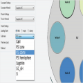
In the next years, the use of PSS will further increase due to its high light extraction efficiency. Following this trend, LayTec‘s in-situ metrology software EpiNet 2 can be individually customized for various kinds of PSS. Our users can expand the substrate database by themselves. LayTec‘s Calibration Manual explains how to measure PSS reflectance in different pockets in one single calibration run. If required, LayTec also offers related customer trainings. Once the initial reflectance values of the PSS substrates are uploaded, the operator can choose the needed substrate in the RunType‘s Material Spec window (Fig. 1). As a result, all PSS wafers can be monitored with the same accuracy as standard sapphire substrates.
Continue reading →
 2013-03-20
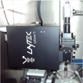
A major challenge of in-situ metrology on single-port reactors with small viewport geometries is the combination of curvature measurements by a blue laser with reflectance measurement at 405 nm. The blue laser is a must for patterned sapphire substrates (PSS) and double-side polished substrates. The 405 nm reflectance is indispensable for monitoring of InGaN MQW growth. Until now, it was impossible to have both features for reactors with only one small optical access because of the cross-talk effect. The new optical and electronic design of EpiCurve® TT eliminates this problem.
Continue reading →
 2012-12-14
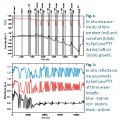
The challenges of GaN growth on Si(111), especially for LED growth, are well known and meanwhile controllable. Cooldown-assisted layer cracking as a result of high tensile stress can be prevented and crystal quality can be enhanced by sophisticated interlayers. Numerous institutions worldwide are already using LayTec‘s EpiCurve TT with advanced curvature resolution for high quality GaN devices on large scale Silicon substrates. Now, this experience is being transferred to growth on Si(001) and Si(110), because GaN based power electronics can be easily in...
Continue reading →
 2012-06-15
On June 11th, 2012, LayTec received the “Aurora Award 2012” in the category “The Best LED Test Equipment” for its latest product, Pyro 400. LEDinside, a Business Division of TrendForce Corp., granted the Aurora award to honor outstanding products for the LED industry. Tom Thieme, LayTec´s general sales manager, received the prize at the Aurora award ceremony that took place in conjunction with the recent LEDforum Guangzhou, China. Thomas Zettler, LayTec´s CEO & president, stated: “We are very proud...
Continue reading →
2012-06-08
LayTec announces that Lextar Electronics Corp., a major LED producer with headquarter in Hsinchu/Taiwan, has qualified LayTec´s GaN surface temperature measurement tool Pyro 400 for its GaN LED production. Mr. Johnson Wang, the department manager of “EPI Engineering/Manufacturing” who was responsible for the Pyro 400 product qualification process, stated, "With Pyro 400 we can now better control the later emission wavelength of the LED already during growth. The qualifications tests have proven that the surface temperature of the G...
Continue reading →
 2012-02-23
It has become a good tradition: November, 29th and 30th 2011 for the 8th time LayTec held its private seminar in Tokyo and Nagoya, Japan. New in-situ measurement approaches for multiple applications as well as product news were presen¬ted.
Prof. Sugiyama of University of Tokyo reported on successful strain compensation of InGaAs/GaAsP multiple quantum wells (MQWs) using both EpiRAS and EpiCurve® TT for novel solar cell applications on GaAs. Interestingly, the H2-purging and subsequent As-/P-stabilization of the InGaAs surface di¬rectly inf...
Continue reading →
2011-12-05
For the third time series LayTec was awarded with Deloitte’s Technology Fast 50 Award for Germany and the Deloitte’s Technology Fast 500 EMEA Award. With a sales growth of 1062% in the period 2006-2010 LayTec achieved place 8 in Germany and place 144 in the area of Europe, Middle East and Africa among the fastest growing technology companies! CEO, president and founder of LayTec, Dr. Thomas Zettler, explains the successful concept: „To receive this award three years in succession shows that we have successfully positioned LayTec in the ...
Continue reading →
2011-11-30
For the third time in series LayTec was awarded with Deloitte’s Technology Fast 50 Award for Germany and the Deloitte’s Technology Fast 500 EMEA Award. With a sales growth of 1062% in the period 2006-2010 LayTec achieved place 8 in Germany and place 144 among the fastest growing technology companies in Europe, the Middle East and Africa! CEO, president and founder of LayTec, Dr. Thomas Zettler, explains the successful concept: „To receive this award three years in succession shows that we have successfully positioned LayTec in the marke...
Continue reading →
2011-09-28
LayTec AG, leading manufacturer of in-situ metrology for MOCVD processes, announces that it has acquired the majority of tangible and intangible assets of Optical Reference Systems Ltd (ORS). ORS Ltd, former competitor of LayTec, entered liquidation in August 2011 after a extended period of difficult trading conditions. Thomas Zettler, CEO & president of LayTec, stated: “The R&D team of ORS did a great job du¬ring the last 3 years in developing complementary metrology technologies. These technologies now will be integrated into LayT...
Continue reading →
 2015-03-13
 2014-11-14
 2013-03-20
 2013-03-20
 2012-12-14
 2012-06-15
 2012-02-23