 2013-03-20
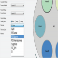
In the next years, the use of PSS will further increase due to its high light extraction efficiency. Following this trend, LayTec‘s in-situ metrology software EpiNet 2 can be individually customized for various kinds of PSS. Our users can expand the substrate database by themselves. LayTec‘s Calibration Manual explains how to measure PSS reflectance in different pockets in one single calibration run. If required, LayTec also offers related customer trainings. Once the initial reflectance values of the PSS substrates are uploaded, the operator can choose the needed substrate in the RunType‘s Material Spec window (Fig. 1). As a result, all PSS wafers can be monitored with the same accuracy as standard sapphire substrates.
Continue reading →
 2013-03-20
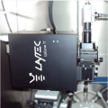
A major challenge of in-situ metrology on single-port reactors with small viewport geometries is the combination of curvature measurements by a blue laser with reflectance measurement at 405 nm. The blue laser is a must for patterned sapphire substrates (PSS) and double-side polished substrates. The 405 nm reflectance is indispensable for monitoring of InGaN MQW growth. Until now, it was impossible to have both features for reactors with only one small optical access because of the cross-talk effect. The new optical and electronic design of EpiCurve® TT eliminates this problem.
Continue reading →
 2013-03-20
 2013-03-20


