 2026-05-22
EV Group (EVG), a leading provider of innovative process solutions and expertise serving leading-edge and future semiconductor designs and chip integration schemes, today announced that it will showcase its latest solutions for heterogeneous integration and advanced packaging at the 2026 IEEE Electronic Components and Technology Conference (ECTC), taking place May 26-29 in Orlando, Fla. These solutions include EVG’s GEMINI® FB production wafer bonding systems, the EVG®40 D2W die-to-wafer overlay metrology system, the IR LayerRelease&...
Continue reading →
 2013-12-04
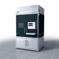
EV Group (EVG), a leading supplier of wafer bonding and lithography equipment for the MEMS, nanotechnology and semiconductor markets, has introduced the EVG®720 automated UV nanoimprint lithography (UV-NIL) system. Providing full-field imprint lithography with an integrated soft stamp/template fabrication capability, the EVG720 system enables throughputs of more than 60 wafers per hour with the lowest cost of ownership (CoO). Capable of printing nanostructures as small as 40 nm in diameter over a large area in volume production, the EVG720 system is ideally suited for use in manufacturing optics, photonics, LEDs, and other bioMEMS devices.
Continue reading →

 2026-05-22
 2013-12-04


