Developing cost-effective methods for transferring Micro LEDs is critical for the commercialization of Micro LED display technology. How to accurately assemble numerous tiny sized Micro LEDs to targeted places efficiently has been one of the biggest challenges for worldwide Micro LED technology developers.
Uniqarta, a U.S.-based startup who focuses on developing innovative assembly methods for integrated circuit (IC), has shared with LEDinside how its laser-based transfer technology can be applied for Micro LEDs. Its article, titled “Laser-Enabled Extremely-High Rate Technology for μLED Assembly,” won the second place in the Micro LED Technology Research Contest. LEDinside was pleased to have a face to face interview with Ronn Kliger, CEO and co-founder of Uniqarta, to talk about the uniqueness of the technology and its current progress.
Kliger shared with us how the assembly method was developed in the very beginning. The technology was invented in the 2008-2013 time period, before the establishment of the company, by Val R. Marinov, a professor at North Dakota State University, who then founded Uniqarta with Kliger in 2013 to commercialize the technology. Instead of Micro LED, the technology was initially built for transferring RFID chips. Then by 2016, Kliger and Marinov decided to change their focus from RFID to LED including Micro and Mini LED applications.

(Ronn Kliger, CEO and co-founder of Uniqarta)

(Val R. Marinov and Ronn Kliger; Image: Uniqarta)
Difficulties for Laser transferring Micro LED and Mini LED
After shifting the focus to LEDs, Kliger noted that it is necessary to customize the technology and indicated three challenges for adopting the technology to Micro LED. The first challenge, which comes before the transfer, is to move Micro LEDs from epitaxy wafer to carriers. The second challenge is to figure out how to place them accurately onto targeted substrates, as the thickness of Micro LED chips is only about 6 μm, as small as a piece of dust. The final challenge involves finding a way to connect the tiny sized Micro LEDs to a circuitry. Uniqarta’s laser transfer method focuses not only on the transfer process, but on a total solution which tackles all three challenges, addressed Kliger.
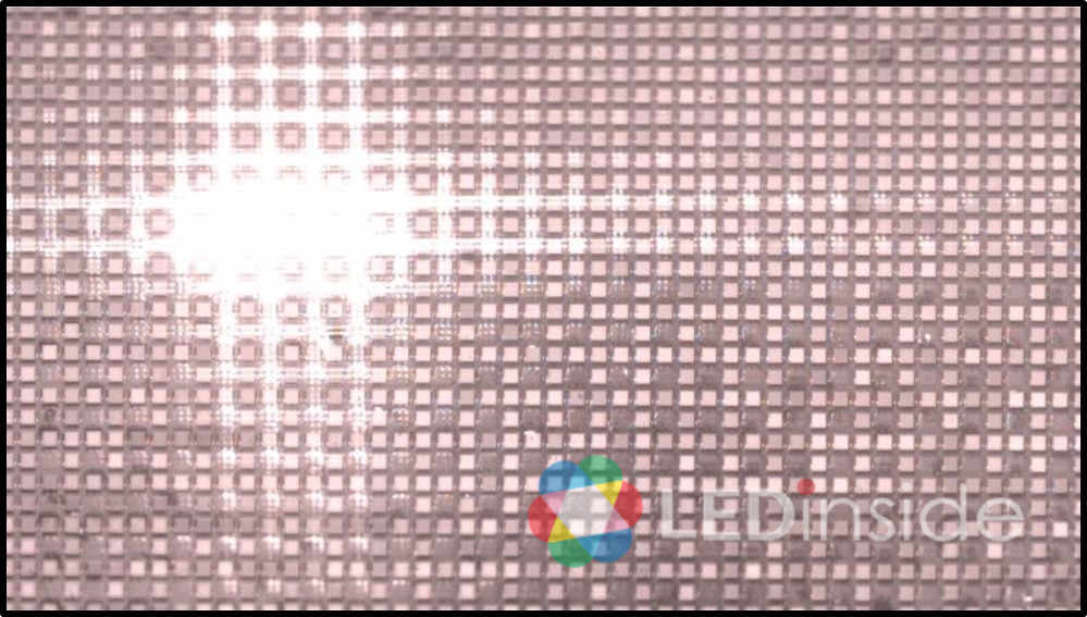
At the moment, the smallest size which Uniqarta’s laser technology can process is 10μm whereas the transfer solution is able to transfer 14 million units per hour with deviation within 6 μm. The company has continued to optimize the technology, according to Kliger.
Currently Uniqarta put more focus on applying the technology for Mini LED instead of Micro LED as the market for Mini LED products is expanding.
Although the technology requirements for Mini LED and Micro LED are similar, we normally consider the technology for Micro LED to be more complicated. However, Kliger noted that there is one thing that is actually more difficult for Mini LED. According to Kliger, the current chip dicing process for Mini LED leads to spacing errors between LEDs. Processing the laser transfer while adjusting and correcting these errors is one factor that can make the Mini LED transferring process complicated.
The laser transfer solution can also be used for the sorting and binning process. Kliger explained that the technology of Uniqarta allows them to follow the sorting map provided by its clients for transferring only the desired LEDs in high speed compared to the conventional pick-and-place method.

(Image: Uniqarta)
The Uniqueness of Uniqarta’s laser transfer method
Speaking of laser transfer technology, Kliger explained that using laser to transfer chips from a carrier material to a target substrate has been a well-known technology. However, previous approaches have used a laser to ablate a release layer bonding the chips to the carrier to release them. These methods are not suitable for Micro LEDs as it is difficult to manage the transfer accuracy and the chips can be damaged by the laser or affected by the residue of the release layer material.
The technology developed by Uniqarta is different from other methods. Kliger addressed that the uniqueness of Uniqarta’s laser transfer technology is that during the laser transfer process, a special material, named a dynamic release layer (DRL), is affected by a laser pulse in a manner that creates a blister to push off the chips without rupturing it. Through applying the dynamic release layer, the transfer process is able to minimize placement errors while protecting LED dies from laser.
Furthermore, Uniqarta combines multiple and single laser beams to select dies during the transfer process to flexibly remove bad dies and place in good ones. By switching between different laser modes, Uniqarta could transfer LEDs efficiently and accurately.

(Image: Uniqarta)

(Image: Uniqarta)
Current Applications and Progress of the Laser Transfer Technology
Uniqarta has been working with industry partners including an LED manufacturer and an equipment producer to implement its innovative technology.
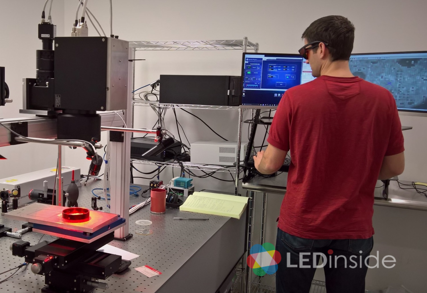
With the collaboration with its equipment maker, Uniqarta will provide equipment utilizing the laser transfer method to end users.
According to Kliger, the first application of the technology will be Mini LED die sorting, which is expected to enter the mass production phase by the beginning of 2020. Afterwards, there will be applications for backlight units and fine pitch displays. With these two applications, Kliger mentioned that Uniqarta will also provide solutions for the electrical connections of LEDs which its clients can apply on the targeted PCB boards before the laser transfer process.
Comments from the judges
Judges at the Consortium for intelligent Micro-assembly system (CIMS) at ITRI considered Uniqarta’s transfer technology feasible and wished to confirm the bounding method of the materials. Meanwhile, judges of National Chiao Tung University underlined the high speed transferring achieved by the method. They both highlighted the originality of the technology and look forward to its future development in both Mini LED and Micro LED.
See full paper: Laser-Enabled Extremely-High Rate Technology for μLED Assembly


 CN
TW
EN

