As one of the most important next generation display technologies, Micro LED performs excellently and can be widely applied in wearables, mobile phones, automotive displays, AR/VR, video wall (digital display), TV and others. For solving the technology bottlenecks of Micro LED, the development of technology relies on cooperation between different companies with their expertise in equipment, materials, panels and brands.

Dr. Ajit Paranjpe, CTO, Veeco Instruments
LEDinside was honored to interview Dr. Ajit Paranjpe, Senior Vice President and CTO of Veeco, to learn the current difficulties of developing epitaxy for Micro LED.
According to Ajit, achieving wavelength uniformity and low defect density to reduce production costs are key factors to successfully apply MOCVD in Micro LED technology. Less than 10 dead pixels are allowed in a display to fulfill the general standard of the display industry. Thus, the yield of LED epitaxy must be very high to reduce the possibility of dead pixels. Currently, Veeco can control the defect density on epitaxy to less than 1 defect per centimeter square.
Sorting and binning are the methods to enhance wavelength uniformity for conventional LEDs. But Micro LEDs are too small to be sorted and binned; therefore, the uniformity of LED epitaxy is even more critical. The requirement for epitaxy in conventional LEDs is around 8-10nm. In comparison, the general requirement of color uniformity for displays is to reach 1-2nm across the display depending on the type of display. It is impractical to achieve a wavelength uniformity of 1-2nm across the wafer. With the appropriate transfer technology, the uniformity requirement of MicroLED can be relaxed to 3-5nm across the wafer. This 3-5nm uniformity requirement can be met using advanced MOCVD tools. Thus, closer collaboration is required between MOCVD epitaxy and transfer technologies.
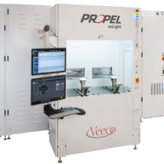
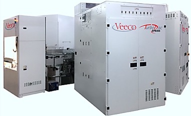
Aside from the performance of products, LED manufacturers also need to consider their operation cost. Veeco has been helping them to reduce the cost of ownership with its equipment and has launched two MOCVD systems, Propel GaN and EPIK 868, for optimizing the operation to meet the demands of the market. The Propel GaN is a single-wafer reactor MOCVD platform for 200mm (8-inch) wafers while the EPIK 868 is a batch MOCVD system for 150mm (6-inch) wafers.


(Source: VEECO)
Ajit noted that Veeco can reach 90 percent yield to produce 8-inch GaN on Si LED wafer with 3nm wavelength uniformity. The feature of GaN on Si LED wafer is that the substrates can be removed easily for wafer bonding. Combined with color conversion technology such as quantum dot, the advanced LEDs will be able to perform full color images, providing improved resolutions for successful application in the HUD projector market.
Ajit also shared his observations on current requirements for Micro LED technology and products. He reckoned that adopting Micro LED will lead to better display quality and that production costs will be reduced in the long run. For HUD, Micro LED will enhance brightness and widen the viewing angle to improve field of view for drivers. Micro LED can also provide higher brightness for AR and VR applications. He added that large-size TVs (bigger than 75-100 inches) will be the sweet spot to adopt Micro LED technology with mobile phones being the last market opportunity as they require high resolution and lower cost.
Veeco has been working with worldwide manufacturers to provide its MOCVD technology for Micro LED manufacturing. Moreover, in addition to MOCVD equipment Veeco also offers innovative technologies such as lithography, ion beam, MBE, ALD, etc. as well as global support and services for production processes to solve specific technical and manufacturing challenges facing the industry.
Author Roger, Joanne / LEDinside


 CN
TW
EN


