Throughout the development of Micro LED, the next generation display technology, cross-industry integration has always been a key. Worldwide chip vendors, panel manufacturers, process technology providers and systems suppliers and others invariably sought collaboration with each other to fully leverage their technological strengths and accelerate their way along the roadmap of Micro LED technology. Among them, equipment solution providers are no doubt the unifiers of processes and technology in each stage along the chain, from upstream chip manufacturing all the way down.
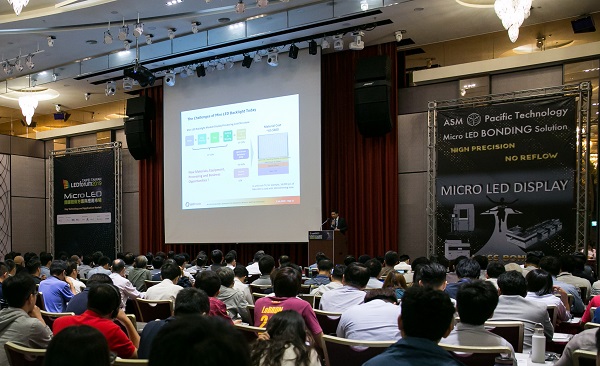
If chip and panel manufacturers are the actors bringing Micro LED technology to commercial center stage, then equipment makers are the workers behind the scenes integrating resources and supporting the performance. They may not enjoy much fame, but they do play a critical role. Micro LEDforum, the grand occasion held every year by LEDinside, welcomed a number of equipment providers to share different solutions for transferal, bonding, inspection and repair.

(Micro LEDforum gathered experts in the industry)
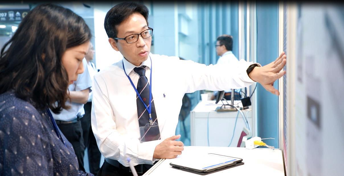
During the event, LEDinside was privileged to interview ASM Pacific Technology (ASMPT), who specializes in post-process equipment for semiconductors. Jonathan Ku, Sales Director of ASMPT gave us a detailed explanation on how their process equipment solutions support transfer and die bonding technology and accelerate the commercialization of Micro LEDs.

(Jonathan Ku, Sales Director of ASMPT, Introduced technology solutions for Mini LED and Micro LED)
Targeting Speed and Yield, ASMPT Provides Solutions for Micro LED and Mini LED
“The greatest challenge for Micro LED production faces still lies in the number of chips,” said Ku in connection with the Micro LED technological roadmap. He pointed out that displays in the past only required 50 to 500 chips for traditional LEDs, but for Micro LED displays, 24 million chips are needed. Thus it is definitely imperative to come up with sped up transfer technology.
It is also paramount to ensure accurate transferal of chips in order to meet the yield demands of the processes to follow. As an equipment provider, ASMPT is up to the task to meet the demands of customers in providing such transfer equipment that satisfies both speed and accuracy requirements. This will, in turn, help customers optimize process efficiency and reduce production costs, putting them further down the road to mass production.
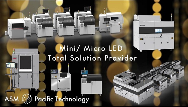
ASMPT’s completed product lines may solve each of the process predicaments faced in Micro LED, Mini LED backlight, Mini LED RGB module and other technologies.
Speaking about Mini LED backlight technology, which has just begun entering the market, Ku noted that this is the technology with the most ease of entry, as traditional pick-and-place approach can easily achieve this. But ASMPT’s strength lies in its ability to provide a high-speed solution. The AD 420 automation system is already seeing usage in current processes for mini LED backlight products.
As for Mini LED RGB display modules, it is essential not only to keep up the speed, but also to improve uniformity in chip arrangement to maintain color uniformity. With conventional techniques, it was difficult to control location, angle and flatness of chips during reflow process. However, ASMPT fully recognizes the requirements for Mini LED RGB and Micro LED display module and has developed AD300Pro which enables mass transfer and bonding. This exclusive solution obviates the need for LED chips to go through reflow, ensuring XY grids and horizontal align for LED chips, making it easier to oversee the evenness of full color RGB displays.
In addition, the Micro LED solution by ASMPT is able to achieve 10,000 Micro LED chips per transfer, whereas bonding efficiency is 80,000 per run. Furthermore, ASMPT’s patented soldering tip is able to ensure the uniformity of the chip even under high temperatures. The technology is capable of achieving an accuracy within 2 μm under a temperature of 350 degrees Celsius or within 1 μm under room temperature. The bonding takes place in ASMPT’s proprietary reactor with chip protection intensified by Nitrogen.

(ASMPT's full solutions for Micro LED and Mini LED)
Collaborating Quietly with Global Giants, ASMPT Accelerates Micro LED Mass Production with Fully Automatic Equipment from Epitaxy to Panels
Besides possessing corresponding platforms for Mini LED backlights, Mini LED RGB and Micro LEDs, ASMPT is able to provide solutions with fully automatic production lines that allow for completely automatic transferal between machines. The automatic solution enables process from the feeding of epitaxy wafer all the way down to panel production without manual control. Applications also go from the test sample to mass production commodities.
Two main foci of ASMPT’s Micro LED solution are mass transfer and bonding. The equipment picks up chips from epitaxy wafer following the map provided by the clients, places onto the temporary substrate, and then transfers to the target substrate for bonding. Currently the bonding yield may reach up to 99.99-100%.
“This year at several display shows, customers have already showcased Micro LED products made by our very own equipment,” said Ku. ASMPT have collaborated with quite a few companies for over a year and half with excellent results. However, the company keeps a low profile as most of its clients deploy strike confidential policies.
Ku revealed that current partners include many panel giants from Japan, Korea, China and Taiwan. The range of application for their products covers large-sized displays, phone displays, automotive displays, transparent displays and more. AD300Pro installations are growing in number, with many customers already prepared to implement the equipment in mass production with ASMPT’s fully-automatic solution.
As an equipment provider, ASMPT is optimistic about the opportunities for the market of transparent Micro LED automotive displays and forecasts that the product will hit the market soonest by the end of 2020. As for wearable applications such as AR/VR devices or watches, we may have to wait until 2021 to see end products make their way into the market.


 CN
TW
EN

