The LED industry is gaining increasing attention from the market as the largest consumer electronics company is said to launch several products using Mini LED backlight display technology. LED industry players are looking forward to increasing demand created by the innovative display technology and hope to get away from the dark time of oversupply and low-price competition.
Nevertheless, LED companies can hardly work on their own to create Mini LED and Micro LED miracles. These miniaturized LEDs are only a hundredth or even thousandth of a conventional LED and the amount used for one display could be ten thousand or hundred thousand times more. Take most popular tablet company’s rumored Mini LED product for example, it might adopt around more than 10K Mini LED chips as backlight source. As for a 4K TV Micro LED display, it will take about 24 million LED chips.
With such small size and massive amount, it would not be cost-effective to process Mini LED and Micro LED with traditional technology and equipment. Consequently, equipment suppliers who introduce mass transfer solutions play critical roles on the way of Mini LED and Micro LED commercialization.
Kulicke & Soffa (K&S), the Singapore-based semiconductor package equipment expert, has invested in Micro LED and Mini LED mass transfer equipment development jointly with Rohinni, the transfer technique provider from the U.S. Chan Pin Chong, Executive Vice President and General Manager of K&S Products & Solutions, talked with LEDinside to share how the new equipment PIXALUX, featuring high speed transferring with high accuracy and yield, helps to achieve cost-effective manufacture of Mini LED products, speeding up the pace of volume production.

K&S and Rohinni Build PIXALUX Equipment with Mini LED High Transfer Yield
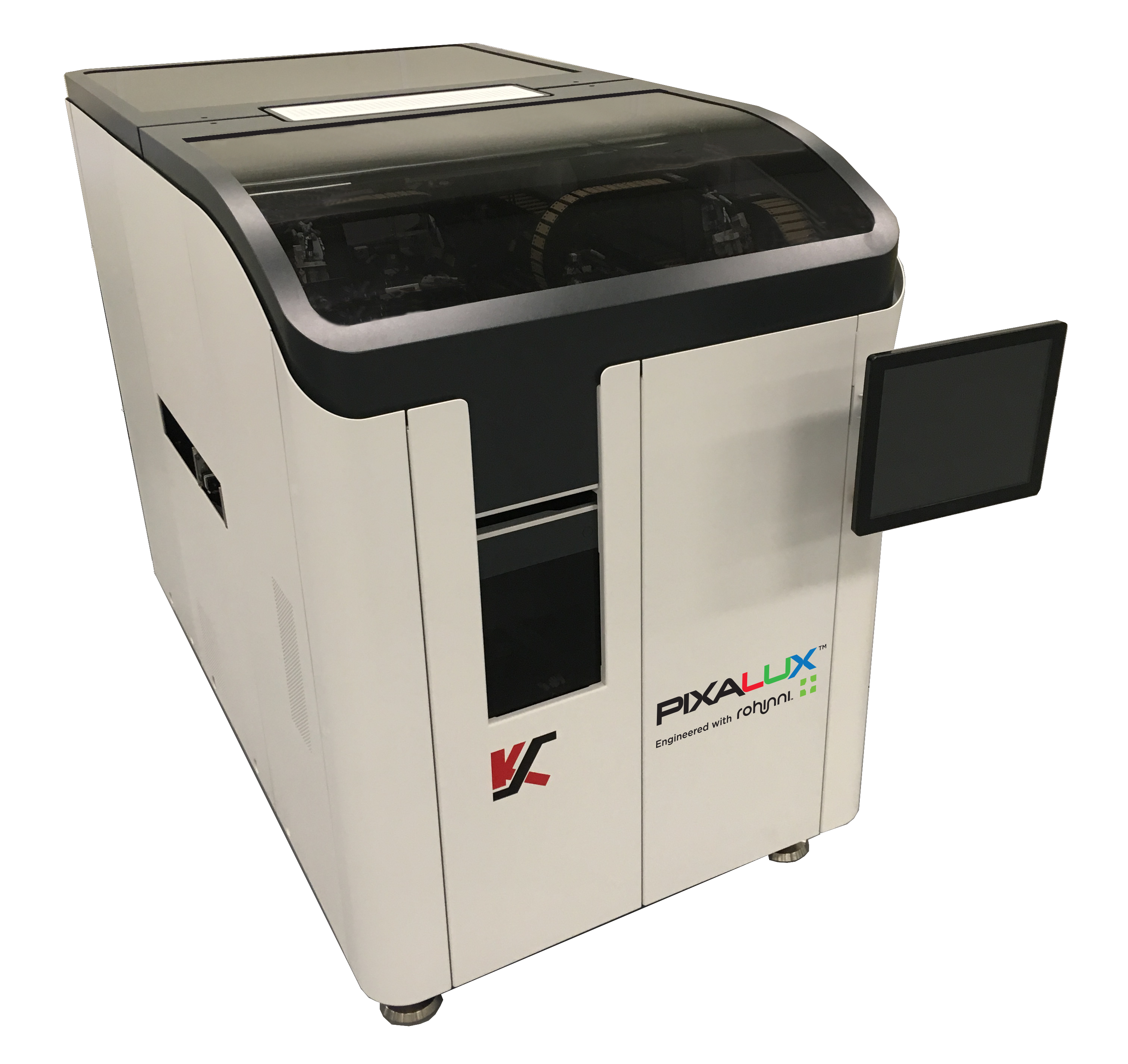
K&S and Rohinni announced their partnership in 2018 for developing mass transfer equipment for miniaturized LEDs. The product PIXALUX is now verified and mass produced.
“The key of reducing cost is transfer speed. PIXALUX is capable of transferring 180,000 LED chips in one hour,” addressed by Chan Pin Chong. Comparing to conventional pick and place technology, the transfer speed of K&S equipment is three to five times faster than traditional die bonder, transferring 50 LED chips per second. The accuracy can be from 10 to 15 µm with high yields.

(Mass transfer equipment PIXALUX; image: K&S)
In addition, robustness of the equipment was also highlighted by Chan Pin as an essential factor of maintaining high yield. The equipment has to run stably during mass production to strengthen speed and yield, which marks edges of K&S. The company has been supplying semiconductor equipment for more than 60 years with not only expertise in hardware but also professionalism in software. By continuously and flexibly adjusting both software and hardware, K&S provides equipment that can operate steadily under various circumstances.
Apart from transfer speed, accuracy and yield, challenges of Mini LEDs and Micro LEDS also show in the process of testing and repairing after transfer. K&S has worked out an automatic solution of replacing defective dies with an R&D partner. Following the feedback of testing, the solution can replace the bad dies with good ones via laser technology.
The solution is currently verified and getting ready for mass production. Combining transferring and repairing solution, K&S is keen to secure high yields for clients.
K&S Plans to Continuously Work on Developing Micro LED Transfer Solution for Chips <50 µm
As for Micro LED, Chan Pin noted that currently the equipment adopts mechanical transfer LEDs based on the technology of Rohinni, which can process chips of about 125 µm. However, if chip size keeps going down, the equipment would be limited. Therefore, K&S is also developing transfer solution that meet the demands of chips under 50 µm.
Despite that transferring Micro LED chips is still challenging and uncertain, K&S has accumulated technology know-hows based on its development in Mini LED solution in the past two years. With the advantage, Chan Pin said K&S plans to reveal a total solution which can process conventional LEDs, Mini LEDs and Micro LEDs in next few years, providing equipment with robustness, high speed, accuracy and cost-effectiveness.
From the viewpoint of an equipment supplier, K&S also noted some application opportunities of Micro LED other than displays. Micro LED could serve as an alternative to photolithography, replacing expensive pre-fabricated photomasks or beam scanning methods. Micro LED lithography technology has demonstrated under 5 µm resolution and could be scaled down even more to sub-micron resolution. Moreover, LiFi communication is another possible Micro LED application.
Mini LED Display Demand to Boom despite COVID-19 Impact
Speaking of the continuous COVID-19 pandemic, Chan Pin said the impact of COVID-19 on K&S has been managed. Global supply chain was inevitably disrupted by worldwide lockdowns in the past a few month but shipments are now resumed since most places had reopened.
K&S’ clients, mostly from Asia, are seeing strong growing momentum in Mini LED and have confirmed their production as scheduled. With PIXALUX’s mass production this year, K&S is seeing a significant growth for the product revenue in 2020 driven by boosting Mini LED demands expecting later this year and in 2021.
“2021 will be a crucial year for Mini LED technology,” said Chan Pin. Once the leading brands debuting consuming products with Mini LED backlight displays, the market acceptance of the advanced quality and performance as well as the increased selling price will be decisive for the technology.


 CN
TW
EN


