Optic inspection is still the mainstream wafer defect detection method in the inspection and metrology field, while E-beam will continue to be a niche market, said KLA-Tencor Chief Marketing Officer Brian Trafas during the opening ceremony of the new training facility held at the company’s Hsinchu branch in Taiwan on May 23, 2014.
Speaking about competitor Hermes Microvision (HMI) projection of expanded e-beam inspection revenue and growing market share, Trafas noted market share ratios have remained the same. While it may appear e-beam market has expanded, “the e-beam (inspection) market share is still around 10 to 15 percent, while optical market overall is still about 85 percent to 90 percent,” said Trafas. He attributed the growing figures in the e-beam sector to overall inspection market expansion.
 |
|
KLA-Tencor CEO Rick Wallace (center) speaking at Taiwan Training Center opening ceremony. KLA-Tencor Chief Marketing Officer Brian Trafas sits to the right of Wallace, while on the left is Norman Chang President of the company’s Taiwan office. (LEDinside) |
E-beam is 1,000 to 10,000 times slower than optic inspection, and only suitable for scanning specific points on a wafer, said KLA-Tencor Chief Executive Officer Rick Wallace. “It takes e-beam up to seven days to scan a single die like those in smartphone chip, while only seven seconds for optical,” said Wallace. The e-beam is most suitable for R&D applications, optics on the other hand are suitable for mass volume detection, and laser is currently the most economic and fastest option.
Physical limits continue to make it difficult for e-beam to make significant speed inspection breakthroughs. “When electrons are close together they repel, but photons don’t,” explained Wallace. Lasers have even greater physical property advantages.
As companies become more cost conscious and demand shorter product development periods, e-beam is too costly for manufacturers to adopt, said Wallace. Many improvements can be made to advance optical inspection resolution. He went on saying some of KLA-Tencor clients have abandoned e-beam because of improvements in the company’s optical technology.
 |
|
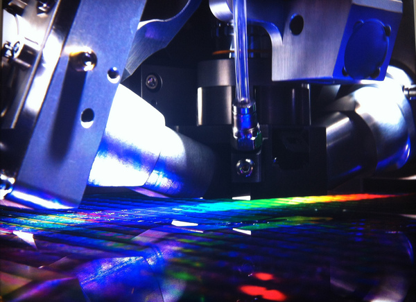
An optical wafer defect inspection system shown on a poster in the Taiwan Training Center hallway. (LEDinside) |
Integrated wafer defection systems still too costly
Asked if system integration is becoming a trend in the wafer defect detection sector, Wallace noted R&D in this area remained few. Most defect detection equipment remain separate tools, but for metrology equipment integration has increased over the years because it allows immediate adjustments on site.
For clients economic tradeoffs are their main consideration when it comes to developing integrated systems, said Wallace. Integrated defect detection systems costs do not always support technology, which may put off clients from asking for integrated systems. Clients also do not always use the integrated detection system. Integrated solutions are best applied to devices that require constant corrections, while a separated single detection tool system can serve more products, he added.
 |
|
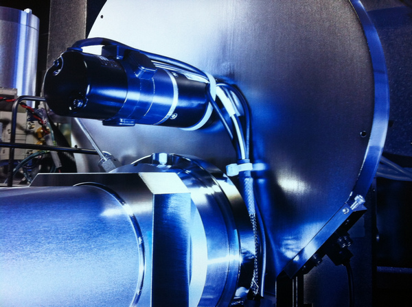
Part of an optical wafer defect inspection system shown on a poster in the Taiwan Training Center hallway. (LEDinside) |
R&D key to future market development
To stay competitive, KLA-Tencor on average invests about 17 percent in R&D. “For semiconductor companies capital is important, but for equipment makers it's R&D,” said Wallace. The company for example invests about US$ 500 million into developing reticle inspection tools, such as the recently launched Teron™ SL650 Reticle Inspection System, before the product is released on the market.
In niche markets with small pool of clients, R&D is especially important for the company to maintain high market share, said Wallace. KLA-Tencor is estimated to have more than a 50 percent market share in the process control and yield management field, according to a Financial Times report. The LED detection inspection sector remains a side project for the company, even though it is being recognized as an emerging market overtime. The adjacent market, which consists of the LED and data storage market applications consists less than five to ten percent of the company revenue, said Trafas.
With the company soon to release its 2014 financial results next month, Wallace projected this has been their second best year ever recorded for the optical inspection market. “The market is growing because every generation semiconductor is becoming more difficult to make, and requires more inspections,” explained Wallace.
[Editorial Notes: Edits were made to correct the e-beam scaning speed of a single die not wafer as previously written.]
(Author: Judy Lin, Chief Editor, LEDinside)


