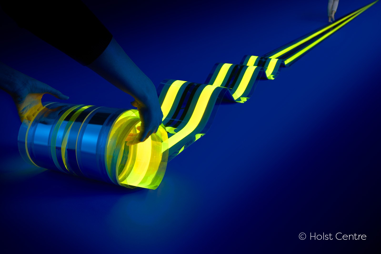
The Netherland-based research center, Holst Centre and Fraunhofer FEP have developed the world's longest single-device OLED which is 15 meters long. The development opens the door to 'endless OLEDs' that manufacturers and designers can then easily tailor to their own needs.
Holst Centre and Fraunhofer FEP worked together through Lyteus, an EU founded public-private partnership organization which brings together leaders in OLED technology from across Europe to create an OLED pilot production line and product development services. Under the framework of Lyteus, the two institutes successfully demonstrated the possibility for continuous production of OLEDs of any length. This both reduces the cost of production and enables "cut-to-fit" lighting for applications such as transportation, architecture and interior design.

(Image: Holst Centre)
It is the first OLED source produced using a unique R2R process that combines the performance of an evaporated OLED stack with solution processing of auxiliary layers. Moreover, the combination improves the process reliability and enables fabrication of devices of any length.
To produce the device, Fraunhofer FEP deposited an indium-tin oxide (ITO) anode onto a protective multi-layer barrier film produced by Holst Centre. The roll was processed at Holst Centre, where slot-die coating was used to structure the anode and deposit the first layer of the OLED stack. Fraunhofer FEP then evaporated the rest of the OLED layers and finalized the devices by lamination of Holst Centre barrier. The resulting devices have a good homogeneity and an efficacy of 15 lumen/W at a light output of 1000 cd/m2.
"Roll-to-roll production promises higher volumes and lower costs for flexible electronics applications like OLEDs. At Holst Centre we have been developing a unique, solution coating roll-to-roll line for 10 years. The 15-meter OLED shows that the technology is now ready for industrialization, and can deliver cost-effective, high-volume OLED production," said, Pim Groen, Program Manager at Holst Centre.
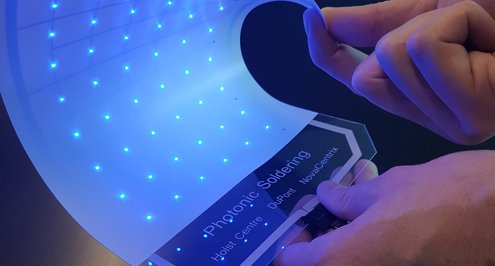
Besides OLED, Holst Centre also announced its partnership with NovaCentrix and their development of photonic soldering, a light-based technique that enable fast, high-resolution integration of silicon components onto flexible foils. Photonic soldering uses intense light pulses from advanced flash lamp systems to cure the solder paste within seconds. Only the solder paste is heated, not the substrate, thus making the technology compatible with low-cost films such as PET. The technique is compatible with roll-to-roll production for cost-effective high-volume production.

(Image: Holst Centre/NovaCentrix)
Francesca Chiappini, scientist at Holst Centre, said, "Flexible hybrid systems require reliable interconnections between the printed and standard silicon components. Our light-assisted technique offers better mechanical stability and electrical connections than existing approaches, and is the only current means for using standard lead-free solder on low-melting-point plastic films."


 CN
TW
EN


