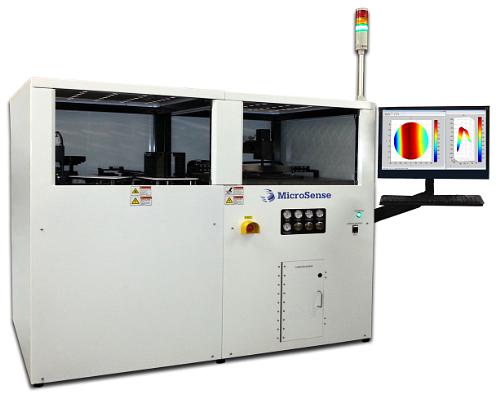
MicroSense, LLC, a leader in non-contact wafer metrology systems, today announced multiple shipments of its new, next-generation automated sapphire wafer metrology tool, the MicroSense UltraMap C200. Designed specifically for high throughput dimensional measurement of sapphire wafers for LED manufacturing, the UltraMap C200 provides throughput of ninety 6" diameter sapphire wafers per hour with lowest cost of ownership (CoO). The UltraMap C200 utilizes MicroSense's novel two sided capacitive sensing technology to measure sapphire wafer geometry including thickness, TTV (total thickness variation), bow, warp, and LTV (local site thickness variation).
 |
|
The MicroSense UltraMap C200A is an automated LED Sapphire Wafer Measurement system based on MicroSense's proprietary two sided capacitive sensing technology. The system measures critical substrate parameters including Thickness, TTV, Bow, Warp and Local Thickness Variation (LTV) with high throughput. The UltraMap C200 is designed for sapphire wafer manufacturers and LED chip makers who require better wafer geometry inspection with higher measurement repeatability, compared to traditional optical metrology systems. (LEDinside/MicroSense, LLC) |
"LED manufacturers typically don't make their own sapphire wafers, so incoming quality control has become a requirement for LED chip makers as the industry continues to migrate from primarily 2" wafers to 4", 6" and 8" wafers," according to David Kallus, Director of Dimensional Wafer Metrology at MicroSense. "LED manufacturers have found high sapphire wafer bow strongly correlates to LED yield loss. The UltraMap C200 utilizes our proprietary capacitive sensing technology and advanced high density wafer mapping algorithms to provide world leading measurement repeatability and throughput."
"Sapphire has become a break out substrate material, and sapphire factories are scaling to capacities unheard of before, driven by the LED and smartphone component markets," continued Kallus. "In order to improve sapphire wafer yields and drive down wafer cost, wafer manufacturers need to measure at more steps in the wafering process. Unlike metrology tools based on optical methods, the MicroSense UltraMap C200 measures sapphire wafers and substrates with any surface finish – as cut, lapped, ground, polished, textured and patterned sapphire substrates (PSS) – without sacrificing wafer throughput or measurement repeatability. Wafer surface condition has no effect on measurement performance."
The UltraMap C200 is available in three versions including tools with robotic loading, robotic loading with cassette sorting and a bench top tool. The UltraMap C200 handles wafers ranging from 2" to 8" in diameter.
Editors and reporters interested in learning more about MicroSense's latest developments in sapphire wafer metrology, MRAM wafer metrology and high resolution capacitive sensors are invited to visit the company's booth # 2143 South Hall in the Moscone Center in San Francisco, California at the SEMICON West show July 8 to 10, 2014.


 CN
TW
EN


