Intentional decomposition of an InGaN layer provides a foundation for high-temperature growth of red-emitting quantum wells
Researchers at the University of California, Santa Barbara (UCSB), claim to have broken new ground by increasing the temperature employed for the growth of red-emitting InGaN LEDs. This breakthrough comes from introducing a relaxed InGaN buffer.
The approach by the West-coast team differs from the norm, which is to grow re-emitting InGaN-based LEDs at a considerably lower temperatures than their green and blue siblings. While growth at a lower temperature enables the higher indium content in the quantum wells required for emission in this spectral domain, it has a major downside: it applies the brakes to adatom mobility, and ultimately drags down efficiency, due to a hike in the defect density and degradation of surface morphology.
The promise of a higher efficiency that stems from a higher growth temperature will be welcomed by developers of displays based on microLEDs. Although AlInGaP LEDs delivers a very high level of efficiency when they have dimensions that are hundreds of microns or more, performance nosedives when scaling, due to the long minority carrier diffusion length. Fortunately, this is not an issue for nitride-based LEDs, due to their reduced surface recombination velocity.
One of the difficulties associated with the fabrication of red-emitting nitride LEDs is the large lattice mismatch between InGaN and GaN. As well as inducing misfit dislocations, the strain that stems from this mismatch reduces indium incorporation through a mechanism known as compositional pulling.
To combat this pulling effect, relaxed InGaN buffers can be introduced that reduce strain and enable higher growth temperatures. Previous work at UCSB has formed such a buffer via an electrochemical etch that porosifies a GaN underlayer. However, according to Philip Chan, spokesman for the latest work, that approach has several weaknesses: it requires complicated processing, it only ensures partial relaxation of the buffer, and it leads to a substantial reduction in the usable area of the substrate.
Chan and co-workers have developed an alternative approach to realising a relaxed buffer, involving intentional thermal decomposition of an InGaN layer.
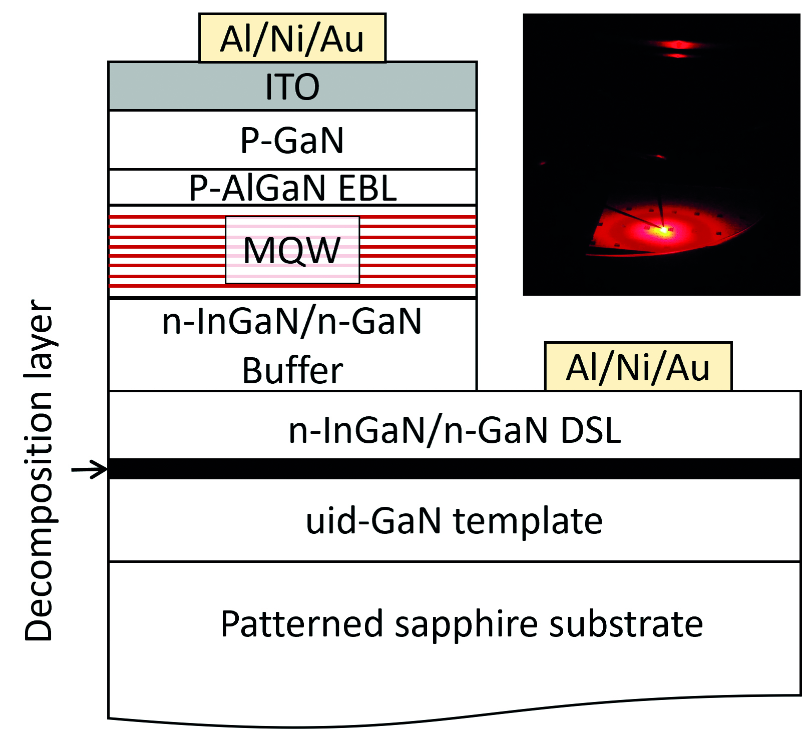
The team's device fabrication began by growing a 3 nm-thick InGaN decomposition layer at 720 °C. Growth of a 4 nm-thick GaN layer at that temperature followed, before cranking the chamber up to 930 °C and adding a decomposition stop layer, comprising five periods of 18 nm-thick n-type InGaN and 2 nm-thick n-type GaN. During this high-temperature growth the high-indium-content decomposition layer decomposed to form voids, allowing the decomposition stop layer to relax and form a template for the LED. On this relaxed platform the team added an InGaN buffer that relaxed, thanks to the compliant decomposition layer, followed by the device (see figure, which shows the decomposition layer with an inset picture of a device operating at 100 A cm-2).
On-wafer testing revealed a shift in the peak wavelength of the LED from 770 nm to 660 nm when increasing current density from 5 A cm-2 to 50 A cm-2. Chan described the magnitude of this shift as “pretty standard”, attribututing it to mainly polarization field screening of the carriers. “Careful control of the doping profile can help to screen this field. But, in general, the commercial viability of red InGaN microLEDs remains to be seen.”
Another concern is the width of the spectral peak. It has a full-width at half-maximum of 69 nm, a value that is not viable for a display, according to Chan. Poor current spreading on the n-side is partly to blame, and should to be easy to fix in future devices.
REFERENCE
† P. Chan et al. Appl. Phys. Express 14 101002 (2021)


