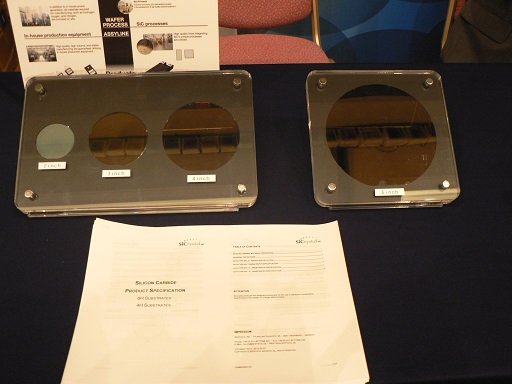
Many SiC-based substrate manufacturers exhibited 6-inch (150mm)-diameter wafers at ICSCRM 2013, an international conference on SiC-based power semiconductors, which took place from Sept 29 to Oct 4, 2013, in Miyazaki, Japan.
Six-inch wafers are the successors to the current 3-4-inch (75-100mm) wafers. Thus far, Cree Inc. has been leading the supply of 6-inch wafers. But companies that are trying to catch up with Cree are expected to launch their 6-inch wafers one after the other from the second half of 2013 to 2014.

Nippon Steel & Sumitomo Metal Corp (NSSMC), which is known for the high quality of its substrates, is currently shipping 6-inch wafer samples, planning to begin volume production in 2014. It intends to provide bare wafers and epitaxial wafers whose epitaxial layers are formed by another company. The quality of NSSMC's 4-inch (100mm) wafer has reached a very high level including its dislocation defect density, and the company is now making efforts to reduce the defect density of its 6-inch wafer to the same level, the company said."Expecting that the 6-inch wafer market will grow, we are discussing whether we should have in-house facilities to form epitaxial layers," NSSMC said.
NSSMC was formed by the consolidation of Nippon Steel Corp and Sumitomo Metal Industries Ltd. Sumitomo Metal Industries was engaged in the development of a technology of growing a SiC crystal by using a solution method. As a result, NSSMC is now developing both the solution method and the sublimation method that was once being developed by Nippon Steel.
SiCrystal AG, which is affiliated with Rohm Co Ltd, will start to ship 6-inch wafers in volume from the end of 2013 to March 2014. The company does not deal with epitaxial wafers and is focused on supplying high-quality bare wafers at low prices, a sales agent for SiCrystal said. Because Rohm quickly evaluates newly-developed SiC wafers, it is easy to receive feedback on the quality of substrate at an early stage, contributing to improving product quality, the sales agent said.
Showa Denko K.K. announced Sept 30, 2013, that it has developed a technology of mass-producing 150mm-diameter epitaxial wafers. The company started to ship samples of the wafers in early 2013. And it started to ship products in October 2013. Though Showa Denko will supply n-type epitaxial wafers for a time, it plans to launch p-type epitaxial wafers in about 2015.


