Micro LED has recently been a high-profile emerging technology in the display industry, where overcoming the existing technical challenges for mass production are the ultimate goal shared by businesses. In Touch Taiwan 2021, leading players such as AUO, Innolux, and PlayNitride flexed their muscles by showcasing various innovative Micro LED applications. In addition to bringing stunning visual experiences, the upstream–downstream partnerships seen in the display event suggests that Micro LED is no longer a “science-fiction” and has stepped closer to the goal of commercialization.

Future Applications of Micro LEDs Are Showcased at Touch Taiwan 2021
At the Touch Taiwan 2021 exhibition, the panel giant AUO unveiled advanced applications of Micro LED display technology related to home entertainment and automotive display. For example, the company worked with PlayNitride to develop a 1.39-inch 338 PPI full-circle Micro LED display featuring the highest resolution density in the world, which can be used with a center console for electric knob applications. Moreover, the gadget boasts a unique curvilinear cutting technique, allowing automobile manufacturing companies to customize solutions for diversified designs of different automotive dashboards, thereby enhancing driving intuitiveness and safety.

1.39-inch 338 PPI full-circle MicroLED display (Source: AUO)
Additionally, the full-circle display module is suitable for mobile devices. Its stunning 338-PPI resolution, ultra-wide viewing angles, and high brightness is likely to inspire applications of wearables in various scenarios. From static and dynamic movements to sunny and snowy weather conditions, the Micro LED product is able to consistently and clearly present information with largely improved visual experiences for users.
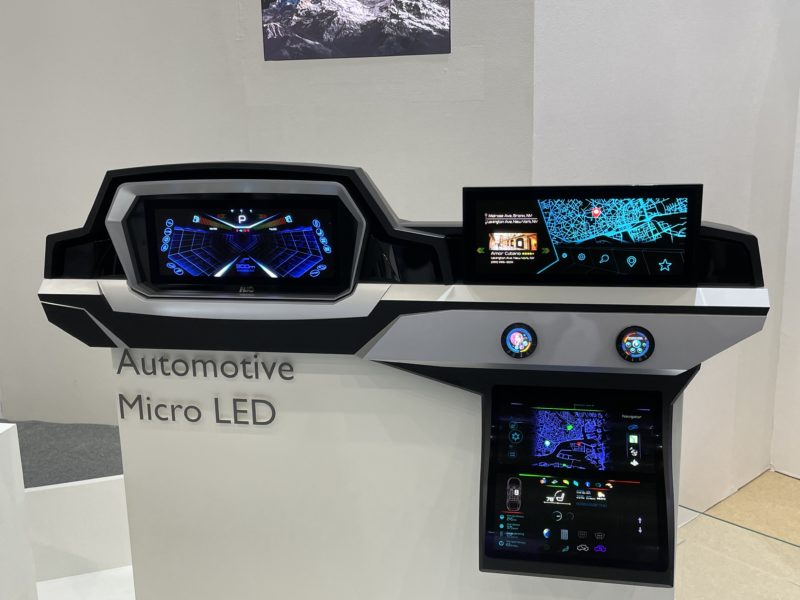
Further, AUO presented a 12.1-inch 169PPI Micro LED display at the exhibition. Adopting color conversion technology, the monolithic monitor boasts excellent weather resistance and stability plus high LED brightness. The said features allow the product to show driving safety information clearly for drivers in sunlight; car dashboards and center consoles are two possible application scenarios of the novel device.

AUO micro LED featured high brightness, high contrast, wide color gamut, fast response and high reliability, making it suitable for various automotive dashboard applications. (Source: TechNews)
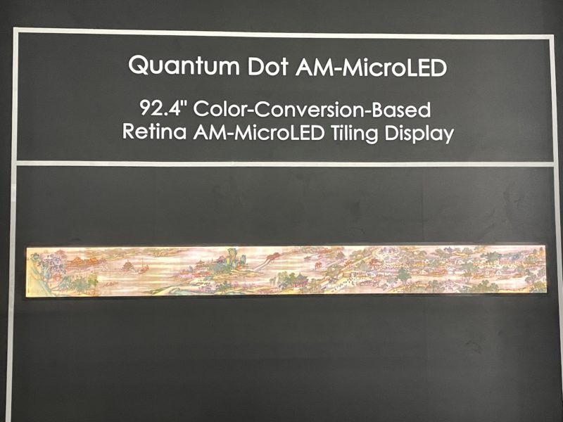
Innolux is not far behind; the panel supplier launched its first 92.4-inch 4K quantum-dot AM-Micro LED seamless tiling display. By overcoming technical limitations faced by LCDs, OLEDs, and fine-pitch LED monitors, the Micro LED product boasts 3D stereo experiences, wide color gamut, ultra-high contrast, smooth dynamic image, retina-level high resolution, and large-scale seamless tiling. The giant display will target markets of 8K cinemas, gaming centers, large security operation centers, virtual museum expos, and large-size displays for elite customers.

92.4-inch 4K quantum-dot AM-Micro LED seamless tiling display (Source: TechNews)
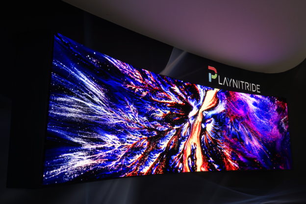
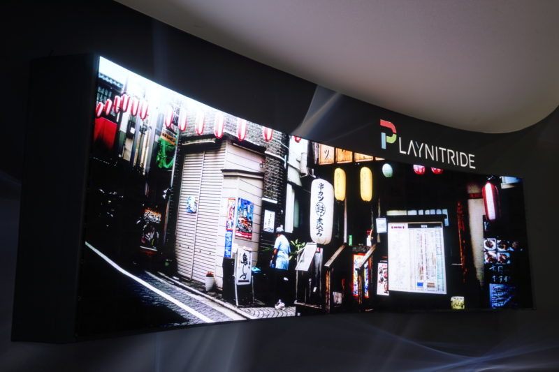
PlayNitride exhibited an 89-inch 5K curved Micro LED display adopting the company’s PixeLED MatrixTM technology with ultra-wide viewing angles, as well as another PixeLED MatrixTM-based SenMirror featuring interactive display. PixeLED MatrixTM is a display technology developed by PlayNitride based on seamless tiling of Micro LEDs. The 89-inch model showcased at Touch Taiwan 2021 comprises 168 matrix modules that are seamlessly tiled to achieve 32:9 ultra-wide display; incorporated with mechanism design, the curved screen features 2,500mm radius of curvature and 2,000 nits of brightness, hence making it a perfect fit for multitasking, gaming, and billboard scenarios.

89-inch 5K curved Micro LED display (Source: PlayNitride)
The smart mirror SenMirror also adopts the PixeLED MatrixTM technology. Utilizing the high brightness and freedom of size design given by the technology, PlayNitride installed gesture sensors in SenMirror, enabling the product to simultaneously serve as a mirror and interactive display.
Mass Transfer Remains the Key to Micro LED Commercialization
Thanks to its wider color gamut, higher brightness, lower power consumption, longer lifespan, and greater durability as well as environmental stability, Micro LED can create amazing visual experiences, which is suitable for various smart applications and highly useful to the display industry. If the existing technical challenges faced by Micro LED are overcome, the trendy technology will be the next-generation display mainstream.
Mass transfer is currently one of the major bottlenecks hindering the development of Micro LED displays. Mass transfer is also the most time-consuming process when producing Micro LED monitors. For example, manufacturing a 4K 3840×2160 monitor requires transfer of more than 20 million Micro LEDs to a backplane. If the speed of mass transfer is not high enough, the process can take up to a few days (even a few weeks). Moreover, a low mass transfer speed and throughput can render Micro LED products costly.
To illustrate, a 65-inch 4K Micro LED TV now costs at least US$100,000; how many people can afford such a luxury in a living room?
Therefore, how to improve the existing mass transfer techniques is a key to mass production of Micro LEDs; that is why numerous leading companies have recently invested in mass transfer, giving rise to various novel approaches. The existing mass transfer technologies include fluidic assembly, laser transfer, roll transfer, and stamp pick-and-place, each aiming at different requirements of customers.
The stamp pick-and-place involves sorting and placing dies using the MEMS array technology. However, the low transfer rate of conventional pick-and-place (approx. 25,000 dies per hour) has posed a big challenge for Micro LED production. Such a low transfer speed indicates that the mass transfer process of a high-resolution (1440×2560) smartphone panel with 11 million Micro LEDs will take 19 days; the process required for a 4K display (3840×2160) would obviously take much longer.
Manufacturers have thus turned their attention to new transfer mechanisms. For instance, Apple Inc. acquired LuxVue, a Micro LED company specializing in mass transfer based on static absorption . Static transfer involves the use of transfer heads releasing static electricity to pick up Micro LEDs from the carrier substrate (or “intermediate substrate”) and release them to the target substrate. Multiple heads then form a static transfer head array that is capable of simultaneous array transfer of Micro LEDs in large quantities, thereby meeting the production requirements of high-resolution displays. Indeed, there are pick-and-place alternatives in addition to LuxVue’s solution, such as Van der Waals transfer printing and electromagnetic transfer.
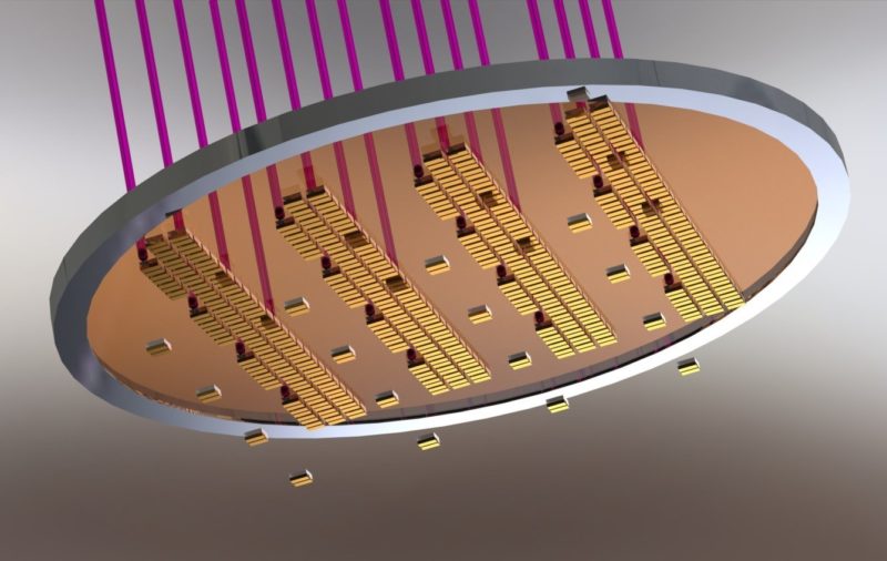
Laser transfer, as its name suggests, refers to the use of laser beams to quickly transfer a large amount of Micro LEDs from the original substrate to the target one. Like other processes, laser transfer comprises several derivatives. The US-based startup Uniqarta, for example, developed the Laser-Enabled Advanced Placement (LEAP) technology that performs mass transfer using either single or multiple laser beams. The highly accurate, ultra-fast laser transfer and die placement system helps Uniqarta to overcome the technical challenges faced by conventional pick-and-place approaches. The non-contact nature of LEAP in large-quantity die placement also accelerates the transfer process.

K&S Acquires Uniqarta to Advance Laser Transfer Technology (Source:K&S)
QMAT, another US startup, adopts the Beam Addressed Release (BAR) technology, of which the principle is similar: using laser beams to quickly transfer an immense amount of Micro LEDs from the original substrate to the target one. Notably, QMAT also proposed a photoluminescence (PL)/electroluminescence (EL) inspection solution to ensure zero ppm defects and high throughput during the mass transfer process. Prior to transfer, an inspection and verification must be performed to ensure that the Micro LED in question is a non-defective good. The solution thus helps reduce subsequent maintenance time and processing cost.
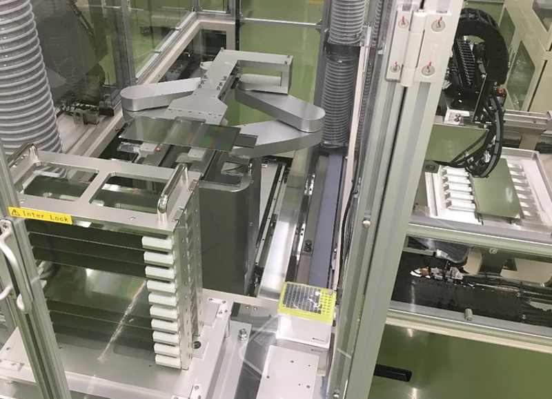
Fluidic assembly is mainly adopted by eLux, which owns a patented fluidic assembly approach that utilizes molten solder interfaces to perform mechanical and electrical connections to an electrode during assembly with suspension fluid being the medium. The economical and efficient assembly process allows Micro LEDs to be quickly captured and aligned with solder joints. Roll transfer is a unique patented technology developed by the Korea Institute of Machinery and Materials (KIMM). Based on roll-to-roll process, the method involves “transcribing” TFT and LED components to a substrate, ultimately fabricating a flexible active-matrix Micro LED (AMLED) panel.

Automated fluidic assembly tool(Source:eLux)
Mass Transfer Inspection Techniques with High Efficiency Also Matter
To enhance the yield rate of Micro LED displays, inspection is another crucial process in addition to mass transfer. As Micro LED products comprise plenty of LED chips, how to accurately and quickly inspect and repair these fine chips has remained a tough issue.
Currently, businesses mainly adopt two types of Micro LED inspections; that is, the PL and EL tests. However, the two have their respective weaknesses. PL enables inspection without contacting LED chips and is less likely to damage the chips, yet the test is not as effective as EL. The EL test, by contrast, performs inspection by setting up electric currents with the LED chip; despite its ability to identify more defects, the test approach might damage the chips because it requires chip contact.
To improve the efficiency of Micro LED inspection, technology developers and equipment manufactures continue to explore inspection techniques. For example, the startup Tesoro Scientific developed a non-contact EL testing approach, which utilizes structures and integrated layers present on carrier substrates to inject currents and test LED components. The testing results can help simulate the yield rate of identified non-defective chips and display well-functioning Micro LEDs, thereby enhancing the yield rate of Micro LED mass transfer.
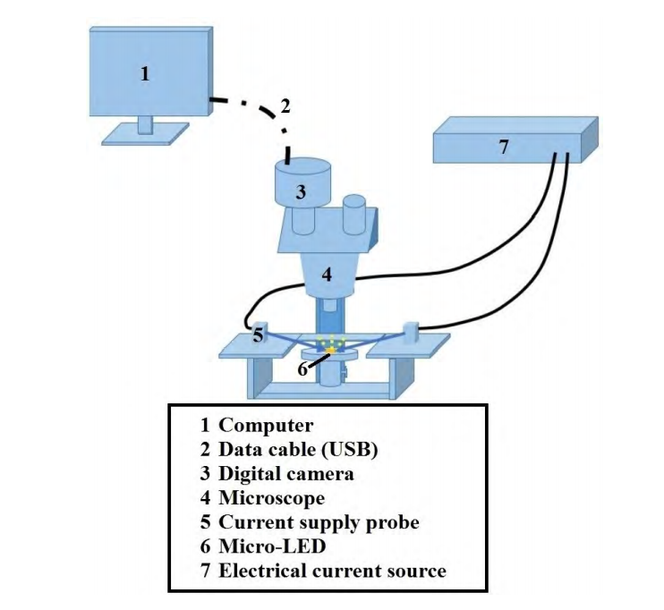
In addition to the PL and EL tests, researchers also seek alternatives by developing novel inspection techniques. For instance, a research team formed by Xiamen University and National Chiao Tung University developed a camera-based microscopic imaging system for Micro LED testing. Featuring a computer, electrical current source, digital camera, current supply probe, and supporting software, the system is able to capture and analyze microscopic images and determine the brightness of Micro LED chips.

The schematic system of microscopic luminance measurement for the Micro LED array(Source:IEEE Access)
In sum, various technical issues for the commercialization of Micro LED displays remain unsolved. However, overcoming these challenges is not impossible but just takes some time. During the Touch Taiwan 2021 event, various potential applications of Micro LED were showcased. The exhibition also demonstrated results of supply chain partnerships, indicating that businesses have strengthened upstream–downstream alliances to surmount the present obstacles. As resources and efforts for research and development increase, technical challenges on mass transfer, inspection, and repair will be resolved one day to create a mature supply chain, making Micro LEDs omnipresent.
(This article is reposted by TechNews)


