As AI moves rapidly into consumer devices, AI/AR smart glasses are emerging as the next major focus of industry attention. From Meta's Ray-Ban Meta smart glasses to new-generation products launched by AR device makers such as Rokid, RayNeo, and Even Realities, and to cross-industry entrants such as Alibaba, Xiaomi, and Li Auto, the industry’s direction is now clear: AI/AR smart glasses are moving from proof-of-concept to scaled adoption.
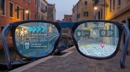
Figure 1. AR Smart Glasses Scenario Illustration
According to information from EssilorLuxottica's fourth-quarter 2025 financial results, sales of the AI smart glasses developed in partnership with Meta exceeded 7 million units in 2025. Driven by global technology leaders and a broad ecosystem of supply-chain participants, the smart glasses market is accelerating toward commercialization and scaled adoption.
AI is making AR smart glasses a more natural and accessible human-machine interface, while AR smart glasses provide AI with the most intuitive hardware platform for everyday use cases. As the convergence of physical and digital worlds becomes an increasingly mainstream interaction paradigm, display technology has emerged as a core determinant of the user experience. It shapes not only visual quality but also device size, power consumption, and wearability.
The current direction of microdisplay technology points toward LEDoS solutions, which offer lower power consumption, higher brightness, smaller form factors, and higher contrast. LEDoS is widely regarded as a key technology path for next-generation AR displays. Yet the industrial reality is more complex: cost remains the decisive variable in determining whether the technology can truly scale.
1. Cost Is the Key Variable for LEDoS Commercialization
In the development of AR smart glasses, wearability, acceptable pricing, and a complete content ecosystem form the three pillars of market expansion. Only when these three dimensions advance in tandem can hardware products meet consumer expectations and enter a phase of scaled growth.
Among existing technology paths, LEDoS is widely seen as one of the most promising solutions for balancing performance and form-factor design. LEDoS offers several key advantages: ultra-high brightness, which keeps AR virtual images clearly visible in complex lighting environments; ultra-compact optical engines, which support thinner and lighter eyewear designs; and lower power consumption, which creates more room for system-level battery life.
The challenge, however, is equally clear. LEDoS optical engines currently account for a relatively high share of total device hardware cost, directly affecting product pricing and market positioning, and to some extent constraining the overall pace of industry adoption.
When the cost of core display components cannot be reduced effectively, products tend to remain confined to premium niche markets, making it difficult to generate the economies of scale needed to support a still-maturing AR ecosystem.
Cost has therefore become the key variable in determining whether this technology path can fully realize its market potential. Only by breaking through the cost boundary of scaled production can end products move into consumer-grade price bands and drive AR smart devices from early trial adoption into true volume growth.
2. CMOS Backplanes Are the Key Cost Driver for LEDoS
A closer look at the LEDoS cost structure shows that the primary cost driver is not Micro LED epitaxy itself, but the CMOS (complementary metal-oxide-semiconductor) backplane.
CMOS backplanes involve complex semiconductor processes, circuit design, and expensive mask sets, resulting in a cost per unit area far higher than that of III-V compound semiconductor epitaxial wafers. At the same time, to meet the requirements of AR near-eye displays for higher pixel density, more sophisticated driving functions, and lower power consumption, CMOS process nodes are continuing to advance toward sub-22nm technologies. These advanced nodes are primarily scaled on 12-inch wafer platforms.
This means that every 12-inch CMOS backplane represents substantial manufacturing value. The central cost question for LEDoS is therefore how to maximize the effective utilization of this high-value 12-inch CMOS area.
In manufacturing, backplane utilization efficiency is determined mainly by three factors: the effective pass-through rate of front-end light-emitting units, the yield performance during integration, and the final usable area ratio. Any compounding losses from epitaxial defects, size mismatch, or integration loss are magnified across the entire 12-inch backplane, creating substantial cost pressure.
In other words, once 12-inch CMOS becomes the value center, the manufacturing logic must center on a single question: how to minimize waste of expensive backplane area.
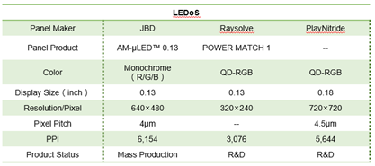
Table 1: LEDoS Microdisplay Panel
3. Structural Limitations of the Conventional W2W Path
In the conventional LEDoS integration path, Micro LED and CMOS backplanes are typically integrated through wafer-to-wafer (W2W) bonding. In volume production, however, this approach has increasingly revealed two structural limitations.
Yield Coupling
Because W2W bonding does not allow effective electrical testing before bonding, manufacturers cannot identify defective areas in advance. As a result, the high-value CMOS backplane must passively absorb yield losses originating from the preceding process steps, including defects and wavelength non-uniformity.
Any localized epitaxial defect can cause the corresponding CMOS area to be discarded together with it. Under this model, expensive CMOS backplanes are effectively forced to pay for upstream yield losses.
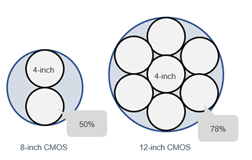
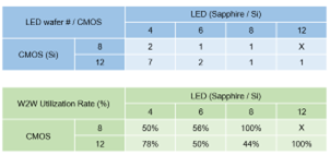
Figure 2: CMOS Backplane Utilization Comparison
Low Utilization Caused by Wafer-Size Mismatch
Today, Micro LED epitaxial wafers are still mainly based on 4-inch and 6-inch platforms, while CMOS backplanes have fully transitioned to 12-inch platforms. This size mismatch inevitably leaves a large amount of backplane area unusable during wafer-level bonding.
For example, bonding a single 8-inch wafer to a 12-inch CMOS backplane leaves backplane utilization at only 44%; bonding two 6-inch wafers to a 12-inch CMOS backplane yields 50% utilization. JBD's current approach, which integrates seven 4-inch epitaxial wafers with a 12-inch CMOS backplane, can reach approximately 78% utilization. Yet even this industry-leading configuration falls short of the ideal.
Against this backdrop, JBD has recognized that structural waste continues to weaken the capacity value of CMOS backplanes and has become a root cause of the cost bottleneck limiting LEDoS commercialization.
4. From W2W to D2W: Reconstructing the Manufacturing Logic
At the same time, the industry faces another key reality: although CMOS backplanes have fully entered the 12-inch era, the scale-up of light-emitting epitaxy remains constrained. Due to differences in material systems, the challenge of controlling epitaxial uniformity, and the technical complexity of large-format bonding, the industrial path for 12-inch light-emitting epitaxy has not yet been truly established. The 8-inch approach also faces potential issues such as low bonding yield. At present, Micro LED epitaxy remains concentrated mainly on 4-inch and 6-inch platforms.
This means that, for the foreseeable future, expanding epitaxial wafer size to match 12-inch CMOS remains subject to considerable uncertainty.
In this context, JBD has chosen the wafer reconstitution path: a die-to-carrier-to-wafer (D2W) scheme. This approach shifts the manufacturing flow from conventional wafer-to-wafer bonding to a sequence of pre-selection, reconstitution, and final integration. It effectively isolates the impact of front-end defects on downstream integration, preventing the CMOS process from passively absorbing unnecessary compounded yield losses and significantly improving both backplane utilization and overall yield.
This shift is not merely a process optimization; it is a reconstruction of the underlying manufacturing logic.
Pre-Selection: Catching Defects Before Bonding
By pre-sorting individual dies, defective areas can be identified and removed before bonding, leaving only clean, process-qualified dies for subsequent steps. This single process step can raise the effective utilization of incoming epitaxial material from approximately 70% to nearly 100%, preventing CMOS backplanes from bearing upstream defect losses.
Full 12-Inch CMOS Bonding Through Lossless Reconstitution
The 12-inch carrier formed through reconstitution can then be fully bonded to a 12-inch CMOS backplane, enabling nearly 100% area utilization.
When backplane utilization approaches full-area utilization, CMOS unit cost can be amortized far more effectively, creating further room for cost reduction in LEDoS microdisplays and optical engines.
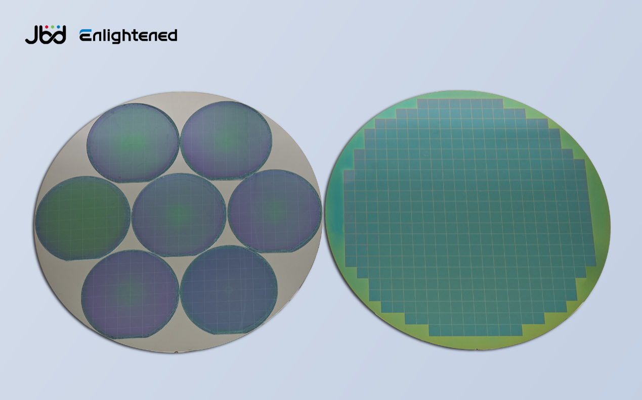
Figure 3: Left, seven 4-inch epitaxial wafers; right, a 12-inch silicon-based reconstructed wafer
As the cost structure continues to improve, end-product prices are expected to decline over time. At the same time, the expansion of scale across the upstream and downstream value chain will accelerate technological evolution, creating a positive feedback loop between technical progress and cost reduction.
5. Redefining Cost Competitiveness Through Manufacturing Reconstruction
As AR smart glasses enter a critical stage of scaling, whether LEDoS can truly break through will depend not only on performance metrics, but also on whether its manufacturing system can support a scalable cost structure.
JBD's transition from 4-inch wafer-to-wafer bonding to a 12-inch reconstitution process is grounded in a deep understanding of industry trends and cost dynamics. By eliminating unnecessary process losses and maximizing the utilization value of CMOS backplanes, JBD has achieved and maintained the world’s lowest unit cost for LEDoS chips. This technology iteration not only underscores JBD's leadership in volume-production technology, but also lays a solid foundation for the commercial proliferation of AR smart glasses worldwide.
When the manufacturing logic changes, the industry’s trajectory changes with it. For the AR smart glasses industry, this marks more than a process upgrade; it is a pivotal step toward unlocking cost-effective scale and broader commercialization.


