The Micro LED Technology Research Contest has received papers targeting all aspects of Micro LED technology development. Aside from mass transferring and methods for full color display, backplane is also a critical factor in the manufacturing process of Micro LED.
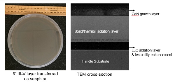
QMAT has focused on the technology of substrate and addressed that advancing substrate helps to solve several issues of Micro LED manufacturing. In its article, titled “Engineered Substrates for High Efficiency Micro LEDs and Commercialized High Volume Manufacturing Production,” researchers demonstrated how QMAT’s EpiMax™ engineered substrates can improve device performance and reduce MOCVD growth time, leading to better quality and efficiency of Micro LED production.

(Author: Dong Lee, QMAT)

(Author, Philip Ong, QMAT)
The article indicates that by using GaN as a seed layer for MOCVD growth, the engineered substrate can enhance device efficiency and limit variability at the desired current density operating point. Moreover, QMAT’s layer transfer technology enables wafers to be effectively utilized as the multiple engineered substrates are made equivalent to original donor substrates.

(Image: Lee and Ong, QMAT)
Advantages of QMAT’s engineered substrate include better device performance, reduced substrate cost and shorter MOCVD growth time. In addition, the substrate can become a print head for selective mass transfer and a functional “Laser-Lift-Off” layer is integrated which allows further ablation process.
Judges from National Chiao Tung University underlined the advantages of utilizing QMAT EpiMax™ substrates and considered the design for testability and printability highly practical for Micro LED manufacturing. The Consortium for intelligent Micro-assembly system (CIMS) at ITRI also appreciated the approach of Laser-Lift-Off which can reduce defect LED dies on the engineered substrates.
See full paper: Engineered Substrates for High Efficiency Micro LEDs and Commercialized High Volume Manufacturing Production


