Germany’s AZZURO Pushing GaN-on-Si LED Wafer to Cut Manufacturing Time and Cost
Germany’s AZZURRO, founded in 2003, focuses on supplying power semiconductor device and LED manufacturers with wafers. AZZURRO owns patents in GaN-on-Si technology. The company’s way is to grow a buffer layer based on GaN material on Si substrate, and then grow a GaN film on the wafer according to different needs of LED and power semiconductor device application. The company noted that currently it can make GaN-on-Si wafer on a 6-inch (150mm) Si substrate, aiming to push it to 8-inch (200mm). LEDinside believes this new manufacturing process will help the migration from the existing LED manufacturing process to silicon substrate manufacturing process. This is LEDinside’s pleasure to have a chance to interview Mr. Erwin Ysewijn, VP Sales & Marketing of AZZURRO to share AZZURRO’s technology and experience.

Mr. Erwin Ysewijn, VP Sales& Market of AZZURRO
GaN-on-Si Technology Bottlenecks and Cost-Down Benefits

Source: AZZURRO
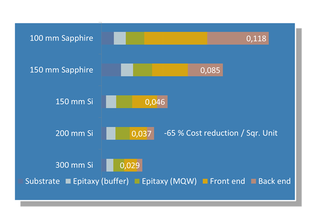
GaN-on-Si technology has been the hot topic in the industry recently, and its technology has been maturing. According to LEDinside, the difficulties lie in materials’ coefficients of thermal expansion – Si substrate and GaN have different coefficients of thermal expansion, which will cause crystal dislocation between these two materials and cause issues such as bow and cracks. Average LED firms will not be able solve these problems by themselves, and that is why GaN-on-Si technology has not reached wide adoption in the industry. However, if the aforementioned problems can be successfully solved LED wafers can be made with GaN-on-Si technology, then the LEDs that are manufactured with GaN-on-Si wafers will produce less thermal and in turn simplify the thermal dissipation designs of LED application products. LEDinside believes it can improve the wavelength uniformity of LED wafers and can drastically cut the production costs and improve yield rate. According to AZZURRO, compared 6-inch GaN-on-Si LED and sapphire substrate LED, GaN-onSi. produced LED cost is 75% less.
According to the GaN-on-Si wafer statistics, in terms of 6-inch (150mm) wafer, the wavelength distribution is as low as 0.764%, a lot better than 4-inch sapphire substrate‘s typical 1.0%. Compared to sapphire substrate, Si substrate is not only more cost competitive but also compatible with the existing Si wafer manufacturing process.
Moreover, when manufacturing flip chip LED, silicon is easier to remove than sapphire, which can shorten the manufacturing process and get better yield rate. If LED manufacturers aim to cut costs and save time, Si substrate is the way to go.
GaN-on-Si Market Development
AZZURRO is optimistic about the technology’s development in Taiwan, so the company has set up technology support and customer service team in Taiwan, helping their clients complete their manufacturing process migration. AZZURRO said that when clients adopt GaN-on-Si manufacturing process, AZZURRO will support them to complete the epitaxy process and predict that clients will need no more than 8 to 16 weeks to do the latter stage of chip manufacture.
Perspective from LEDinside
Looking at the GaN-on-Si market development in 2012, compromised by the technology bottlenecks of large-sized sapphire substrate and the high price of 6-inch sapphire substrate, most LED firms still use 2-inch and 4-inch substrates. However, first-tier LED companies are all developing GaN-on-Si wafers in R&D stage. In addition, European and American companies are speeding up the establishment of 6-inch GaN-on-Si production lines in 2012. Once they start mass production, GaN-on-Si wafers’ price-performance ratio and luminous efficacy will strike a better balance.
LEDinside believes with this new technology developing, it will cut the manufacturing costs and increase production efficiencies in the LED industry. In the meantime, the existing equipment will be able to be used for the new manufacturing process. In the long run, the cost will continue to drop. The question remains: when will the great market demand surge come? GaN-on-Si. LED are here to set a new direction in LED manufacturing.


