Featuring high resolution, high contrast and high brightness, Micro LED is regarded as the “ultimate display technology.” However, due to production difficulties, the technology has not yet entered the commercial market despite that the first prototypes were revealed back in 2012. Recently, driven by leading brands including Apple and Samsung, we have seen more and more Micro LED displays presented. But industry experts forecasted that it would take at least three years for the technology to truly enter the consumer market.
Mass transfer is a notorious challenge for Micro LED display technology to further improve. Different approaches such as transfer stamps, fluidic assembly technology and inkjet printing have been proposed to tackle the bottleneck, but they all suffer from insufficient yield of Micro LED chip processing in the preceding production steps.
ALLOS, the Germany-based GaN-on-Si expert, believes that their advanced GaN-on-Si epitaxy wafer technology is the decisive contributor to overcome the yield issue which currently prohibits Micro LED volume production.
Dr. Atsushi Nishikawa, CTO of ALLOS, shared the technology of ALLOS and explained how the GaN-on-Si wafer can overturn the current Micro LED production process and pave the way for new ecosystem in the industry.

(Dr. Atsushi Nishikawa, CTO of ALLOS; image: ALLOS)
GaN-on-Si Wafer Breaks Limitations of Micro LED Production
ALLOS advocates a new approach for Micro LED display production by creating GaN-on-Si wafer, choosing a different way comparing to the mainstream sapphire-based LED wafer. Dr. Nishikawa explained how GaN-on-Si wafer can be the solution to today’s problems for Micro LED display production.
“Using silicon instead of sapphire will significantly improve production yield and reduce cost,” explained Dr. Nishikawa. He pointed out three advantages of silicon-based wafer for Micro LED display production.
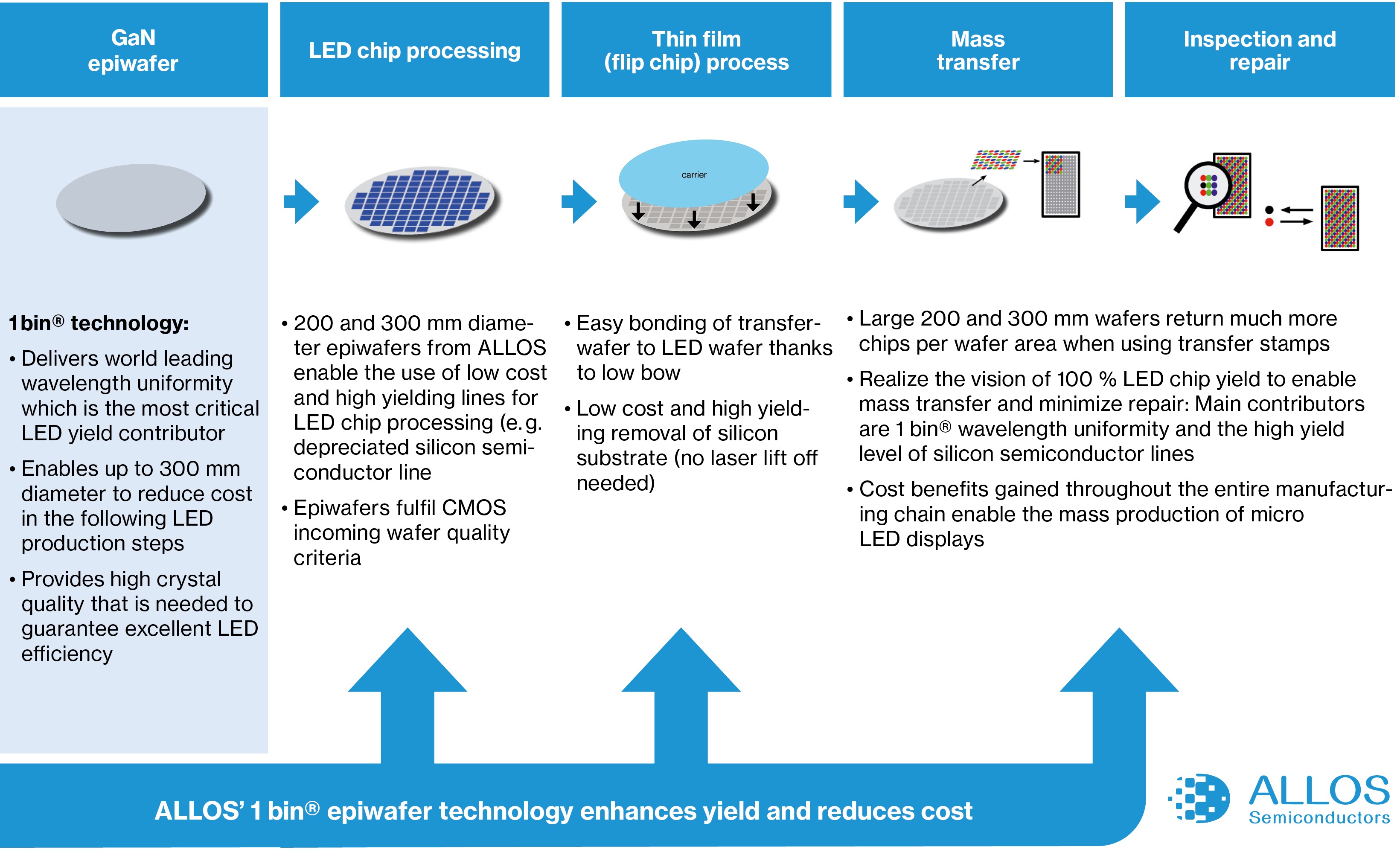
First of all, by adopting silicon-based wafer, involved manufacturers can easily collaborate with silicon foundry to process tiny Micro LED chips with existing semiconductor facilities which offer advanced accuracy. Also, in the case of monolithically integrated micro displays for e.g. AR application, silicon-based LED wafers with bigger diameter can bond directly with CMOS backplane without extra transferring process. Moreover, once the bonding is done, the technology for removing silicon substrate is much more mature comparing to sapphire substrate removal, so that chip makers do not have to bother with the issues of weakening structure or laser lift-off that might impact chip efficiency and yield.

(ALLOS demonstrates how its technology enhance Micro LED production process)
In a nutshell, by utilizing silicon-based LED wafer and semiconductor equipment, most of the current challenges for Micro LED display production - covering mass transferring, mass inspection and driver IC integration - can be addressed significantly better by having chips with much higher yield available.
However, such approach of directly bonding big size wafer and driver backplane does require a much better wafer uniformity, which is the core of ALLOS’ technology.
ALLOS Realizes Reproducibility of 200 mm GaN-on-Si Wafer with High Uniformity
“ALLOS has achieved mass production requirement with 200 mm GaN-on-Si wafer,” highlighted Dr. Nishikawa. He stressed that ALLOS has proved excellent reproducibility for creating 200 mm GaN-on-Si wafer with standard deviation of wavelength uniformity below 1 nm.
Dr. Nishikawa explained the challenges to produce GaN-on-Si LED wafer with large diameter. He noted that the emission wavelength is very sensitive to the growth temperature during multi-quantum wells (MQWs). Even if the temperature changes only slightly during the process, wavelength of wafer will be affected. This is also a challenge for the uniformity of the temperature which is affecting the uniformity of wavelength. What’s more, the wafer also changes its shape during the cooling process and can easily crack. In order to compensate the shape changes during the cooling down, a properly designed amount of strain needs to be induced to the wafer during the process.
Therefore, ALLOS deploys its strain engineering technology to carefully manage the temperature over the entire wafer while designing the perfect curvature for the wafer so that it will be flat and with outstanding uniformity after cooling down.
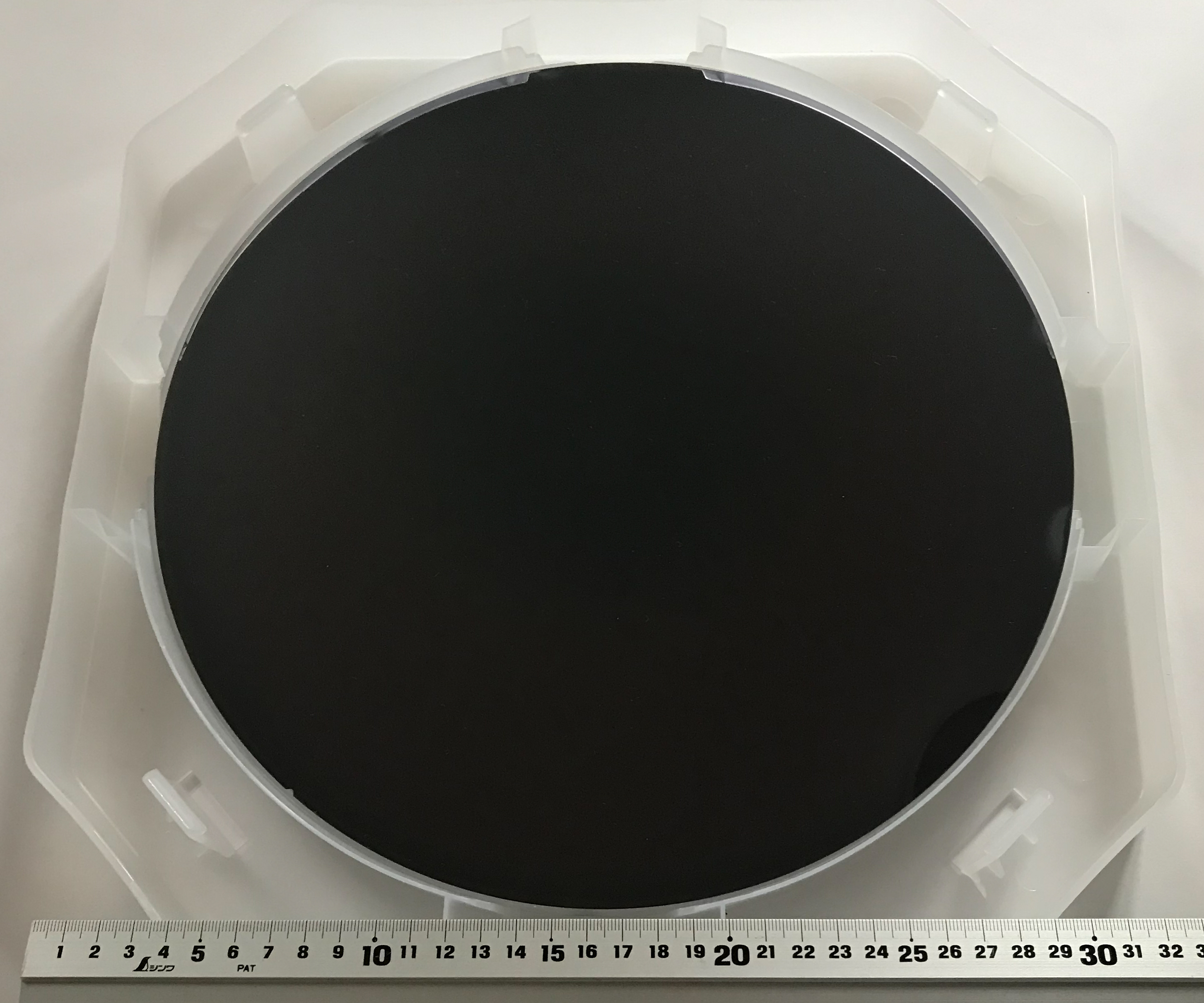
ALLOS is already able to manufacture 200 mm wafer with a uniformity of below 0.6 nm and without a single crack and is working on further improvements. The company has demonstrated the capability of the technology for mass production with reproducibility of < 1 nm. Currently, ALLOS is working demonstrating similar results on its already existing 300 mm wafer technology.

(300mm GaN-on-Si wafer)
Meanwhile, ALLOS is working with KAUST to jointly develop InGaN red Micro LED with GaN-on-Si wafer. The KAUST team announced their achievement in building InGaN red Micro LED with better efficiency earlier this year. The two parties will collaborate to apply the approach to silicon-based wafer to speed up low cost full color Micro LED display production.
GaN-on-Si Wafer Leads to Low Cost Micro LED Display Production with Semiconductor Technology Integration
Speaking of the outlook of Micro LED technology, Dr. Nishikawa emphasized, “Adopting larger wafer and deploying semiconductor equipment will be the key for Micro LED display technology commercialization.”
ALLOS unveiled its capability to achieve crack-free 200 mm wafer with high uniformity that meets the mass production standard and is already adopting it to 300 mm wafer production. Dr. Nishikawa concluded that bigger wafer will lead to lower cost per area and enables the usage of CMOS facilities with enhanced yield and lower cost for mass production, outpacing conventional LED production line.
In fact, utilizing semiconductor facility for Micro LED display manufacture process is a rising trend in the industry with players joining the game. The recently reported Micro LED displays developed by Sharp, for example, were manufactured by semiconductor facilities with technology provided by the Foxconn Group. TrendForce analyst Roger Chu has pointed out before that Apple could be using semiconductor facilities of TSMC to develop new Micro LED processing technology.
Silicon-based, large-diameter wafer technology – like the one of ALLOS – will facilitate the integration of Micro LED and semiconductor technology, offering alternative solutions for innovative Micro LED applications. At the moment, ALLOS is strengthening its partnership with the Micro LED supply chain, aiming to expand the deployment of silicon-based wafer in the industry to enable low cost and high yield Micro LED display manufacture.


 CN
TW
EN


