LEDs have a very bright future.
According to a market research report published by Strategies Unlimited (SU), the high-brightness (HB) LED market, experienced a 93 percent growth rate between 2009 and 2010. In 2009, the global market for packaged HB LEDs was $5.6 billion. In 2010, it grew to $10.8 billion. SU is predicting that by 2015 the global market will be worth $18.9 billion, representing a compound annual growth rate (CAGR) of 11.8 percent.
Despite the positive forecast, there is one element that has the potential to stifle the growth of the LED market: high (and growing) production costs.
The U.S. Department of Energy is expected to release a report stating that in order to compete effectively with the fluorescent lighting market, solid-state lighting manufacturers need to cut the cost per lumen (currently at $18/klm) by 8x to $2.20/klm by 2015
Gaining efficiencies during the manufacturing process is a key method to drive down costs. Larger-diameter sapphire wafers hold the promise of making the manufacturing process significantly more efficient, but they also present challenges to fabricators.
Transitioning from the utilization of a standard 2-inch wafer to a wafer measuring 4-inches in diameter essentially quadruples the available surface area of the wafer. A doubling of the surface area occurs when moving from a 4-inch to a 6-inch wafer, and with every subsequent jump in size comes further substantial increases in surface area.
Unfortunately, theoretical efficiencies gained through the use of larger wafers are drastically undercut if existing manufacturing equipment is unable to cheaply or easily scale up to accommodate the larger form-factors.
Patterned Sapphire Substrates (PSS) serve a dual-purpose role in the LED industry. On the wafer supplier side, they are money-makers. PSS wafers represent higher gross margins than traditionally polished sapphire wafers. On the product development side, PSS-based LEDs are more efficient, more effective light sources.
“The PSS reduces the dislocation density in the GaN (Gallium Nitride) layer and enhances the light extraction efficiency (LEE) from the LED chip by scattering the light confined in GaN layer attributed to the critical angle between GaN (n=2.4) and sapphire substrate (n=1.7) (or air (n=1.0)).”Kazuyuki Tadatomo and Narihito Okada Development of patterned sapphire substrate and the application to the growth of non-polar and semi-polar GaN for light-emitting diodes Proc. SPIE 7954, 795416 (2011);
http://dx.doi.org/10.1117/12.874179
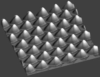
Dry etching is currently the most common method for producing PSS wafers. At this point, the techniques and technology for dry etching, including the inductively coupled plasma (ICP) variant of dry etching are commonplace: lithography exposes a pattern onto the sapphire substrate’s photoresist, which is subsequently anisotropically etched into the crystalline structure via exposure to fluoride-base plasma gas and microwave energy. The resulting, highly uniform and densely packed dome-shaped pattern encourages lateral film growth, resulting in fewer defects and increased light refraction. The LEDs formed using dry-etched PSS wafers produce highly efficient, very bright light.
Dry etching is a very slow process with a low throughput rate. Depending on the type of film used and the depth of the pattern being etched, a standard 2-inch wafer can take between 30 and 60 minutes to etch. Although it is nearly impossible to talk about average rates, given all the possible variables in the process, it is estimated that dry etching rates range between 50nm to 200nm per minute, or 20 minutes per micron.
The dry etch process also does not scale effectively. As wafer size increases, throughput of a dry etcher decreases as fewer wafers fit inside the vacuum chamber. This means more expensive plasma etching tools are required to obtain the same throughput as was achieved on smaller wafers. More tools also come with increased operational costs, such as facilities, maintenance, utilities, and consumables.
In comparison, the high-temperature wet etching process provides the dual advantages of being extremely fast and comparatively much cheaper than dry etching.
During high temperature wet etching, Gallium Nitride (GaN) or Indium Gallium Nitride (InGaN) coated wafers are placed in a tank containing a mixture of etching and buffering agents -- normally sulphuric and phosphoric acids typically in a 1:1 or 3:1 ratio. Prior to submersion, a silicon dioxide mask is spun onto the sapphire substrate via a plasma enhanced chemical vapour (PECVD) process and lithography is employed to expose the desired pattern. Temperatures ranging between 260°C and 300°C are applied to mixture. These temperatures greatly surpass those used in traditional semiconductor fabricating (which typically range between 150°C to 180°C).
Rather than etching rates increasing along a linear scale as the temperature rises, they increase exponentially, Hence a 300°C temperature may have an etch rate that is twice as fast as the etch rate experienced at 260°C. Conversely, researchers have demonstrated that “the etching rate increased linearly when the H2SO volume ratio increased from 0 to 75%.”
Wuu et al. Fabrication of the Pyrramidal Base Sapphire Substrates for High-Efficiency Based InGaN-Based Light Emitting Diodes, Journal of Electrochemical Society 153 (8)G765-G770 (2006)
According to Sinmat’s Singh, high temperature wet etching rates can be measured in microns per minute, with a rate of more than 1 µm per minute certainly being achievable under the correct conditions. He says it is reasonable to expect a standard 2-inch wafer to be fully etched in five minutes.
Natsuko Aota, an Engineer at Namiki Precision Jewel Co. Ltd. is a proponent of the wet etching process and believes in its role as a key cost reducer in LED mass production.
The high temperature wet etching process holds the advantage over dry etching in terms of speed, cost, and scalability. A process tank for a batch of 6-inch wafers, for example, is only slightly more in cost than a tank designed for a batch of 2-inch wafers and can hold the same number of wafers.
Of course, the use of extremely hot chemicals can pose a challenge for manufactures. Chemicals hot enough and powerful enough to rapidly etch sapphire surfaces must be contained and handled safely. At the core of any system is the tank. It must be designed not to react with any of the chemicals, so tanks, such as the Imtec Acculine XE-Series are constructed of high purity, virgin annealed quartz. They contain no plastics that come in contact with the mixture. Built-in temperature sensors feed precise readings back to the systems management equipment. As added safety features, the XE-Series includes a cool down module to house the hot chemistry while it cools and an overflow tank that can hold 120 per cent of the volume of the main tank, in case an accident should occur.
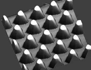
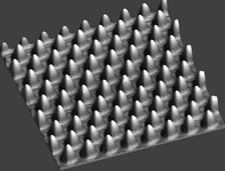
The PSS that results from the high-temperature wet etching process is a significant improvement upon a non-patterned wafer in terms of light extraction and efficiency. The process results in the creation of truncated cone shapes – conical structures with flat tops.

Unfortunately, the flat top surface of the cone poses two significant challenges to those used to working with the dry etching process. The flat topped surfaces act to discourage the lateral growth of film and encourage vertical film growth, resulting in an increased number of defects. Additionally the shape of the structures inhibits efficient light refraction.
Since this is still a relatively new process, research is being conducted into improving the quality of wet etched sapphire wafers. One company undertaking such research is Sinmat Inc., which has developed a method to polish the flat structures thereby producing rounder, more efficient domes – domes that more closely resemble the shape of those produced by the dry etching process.


(Left) Formerly flat, truncated shapes polished and rounded now more closely resemble dry-etched PSS patterns (Right).
Others are investigating the creation of patterns other than cone shapes. At the National Chung Hsing University in Taiwan, researchers created “truncated-triangle-striped patterned-sapphire substrate and a rhombus-like air-void structure at the GaN/sapphire interface to increase the light extraction efficiency. The truncated-triangle-striped patterned-sapphire substrate was fabricated through a wet etching process in hot sulfuric and phosphoric acid solutions. A rhombus-like air-void structure at the GaN/sapphire interface was formed though a wet etching process along a V-shaped air-void structure on the patterned sapphire substrate.” After testing, the researchers concluded that “the [rhombus-like air-void structure LED ]RA-LED has a 65 percent light–output power enhancement, a smaller divergent angle, and a periodic higher light intensity profile compared to a [flat sapphire substrate standard LED] STLED that provides a high external quantum efficiency in Nitride-based LED applications.” Dai et al. Enhanced the Light Extraction Efficiency of a InGaN Light Emitting Diodes
with an Embedded Rhombus-Like Air-Void Structure, Applied Physics Express 3 (2010) 071002
Currently, LED manufacturers have the choice of two very different manufacturing processes. Dry etching creates bright efficient LEDs but does so slowly and with limited throughput. Wet etching is fast and very scalable, but produces LEDs that aren’t quite as effective or efficient. Wet etching, however presents a considerable cost savings over dry etching, even if polishing touch-up work is performed on the wafers to increase light extraction efficiencies. It also scales much more efficiently making the cost savings multiply dramatically as throughput and wafer size increase.
Looking at the financial side, Rajiv K. Singh, Founder and CTO of Sinmat breaks the numbers down like this: “Say you look at a flat substrate, and then you make a patterned substrate, the cost of making a pattern substrate increases the cost by 20 per cent or maybe 25 per cent. The wet etch would decrease that added cost by half.”
Given the combination of per unit cost savings with significantly higher etch-rates, LED Manufacturers and Sapphire Wafer Suppliers need to give high temperature wet etching serious consideration.


 CN
TW
EN

