It has become a good tradition: November, 29th and 30th 2011 for the 8th time LayTec held its private seminar in Tokyo and Nagoya, Japan. New in-situ measurement approaches for multiple applications as well as product news were presen¬ted.
Prof. Sugiyama of University of Tokyo reported on successful strain compensation of InGaAs/GaAsP multiple quantum wells (MQWs) using both EpiRAS and EpiCurve® TT for novel solar cell applications on GaAs. Interestingly, the H2-purging and subsequent As-/P-stabilization of the InGaAs surface di¬rectly influences the resulting bulk strain of MQW structures. He clarified that at least 3 seconds with only TBAs and TBP flow are necessary before TMGa gas flow restarts for GaAsP well growth. Only runs using this technique showed comple¬tely flat wafers after MQW growth (see Fig. 1).
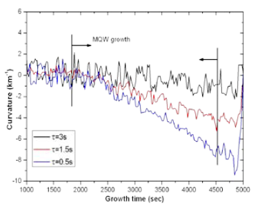
Fig. 1: Variation of cur¬vature in MQWs grown with different surface stabilization time bet-ween InGaAs well and GaAsP barrier growth. Stabilization times below 3s of otherwise strain-ba¬lanced structures result in compressive strain.
Prof. Sugiyama and his team clarified the physical reason of this behavior by RAS investigations of the surface stabilizati¬on process (see Fig. 2).
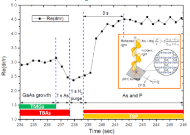
Fig. 2: In-situ Reflec¬tance Anisotropy Spec¬troscopy by EpiRAS showed that a stable mixed P- and As-sur¬face dimer configurati¬on needs at least 3 se¬conds of stabilization time.
Prof. Miyake of Mie University presented high crystal quality GaN on sapphire wafers by controlling overgrowth of stripe-patterned GaN buffers including stripe-voids from former SiO2 masking. The overgrowth of this GaN stripe-void-struc¬ture with a GaN cap layer was optimized by precise control of the anisotropic, aspherical bow of the wafer using an EpiCurve® TT metrology system.
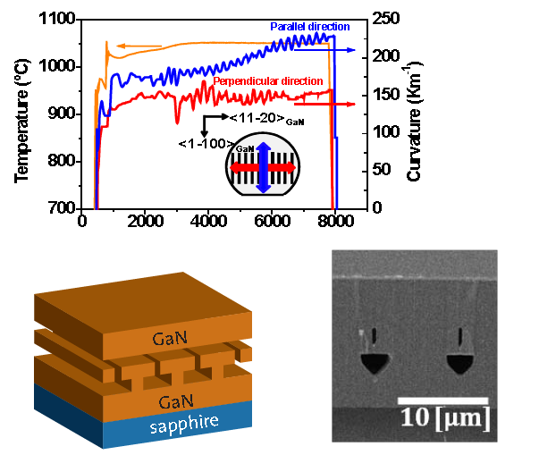
Fig. 3: In-situ curvature measurement in two different directions (blue: parallel to GaN stripes, red: perpendicular to GaN stripes) and temperature measurement during the growth of GaN on a striped GaN/void structure.
Last but not least examples of curvature engineering for GaN on Si devices were presented by Dr. Yuto Tomita of LayTec AG.
Service and Application Engineers wanted!
Due to the largely increased number of LayTec metrology systems in the field we are looking for new service engineers who want to join our customer support team. If you are in¬terested and you have a technical or scientific background in the field of semiconductor epitaxy, modern thin film techno¬logies or optical metrology, please send your application to Mr. Walter Gibas (walter.gibas@laytec.de)


