Researchers based in China report on the fabrication of 270nm-wavelength deep ultraviolet-C (UVC) arrays of micro-LEDs with a view to maskless proximity photolithography [Feng Feng et al, nature photonics, published online 15 October 2024].
The team from Hong Kong University of Science and Technology, Southern University of Science and Technology, Suzhou Institute of Nanotech and Nano-Bionics, comments: “UVC micro-LED arrays are increasingly valued in photolithography and photochemistry as tools for generating arbitrary image patterns and transferring them onto light-sensitive materials like photoresists, eliminating the need for costly photomasks.”
UVC LEDs have previously been developed mainly for virus sterilization applications with a view to high efficiency, extended lifespan and low environmental impact, compared with mercury vapor lamps.

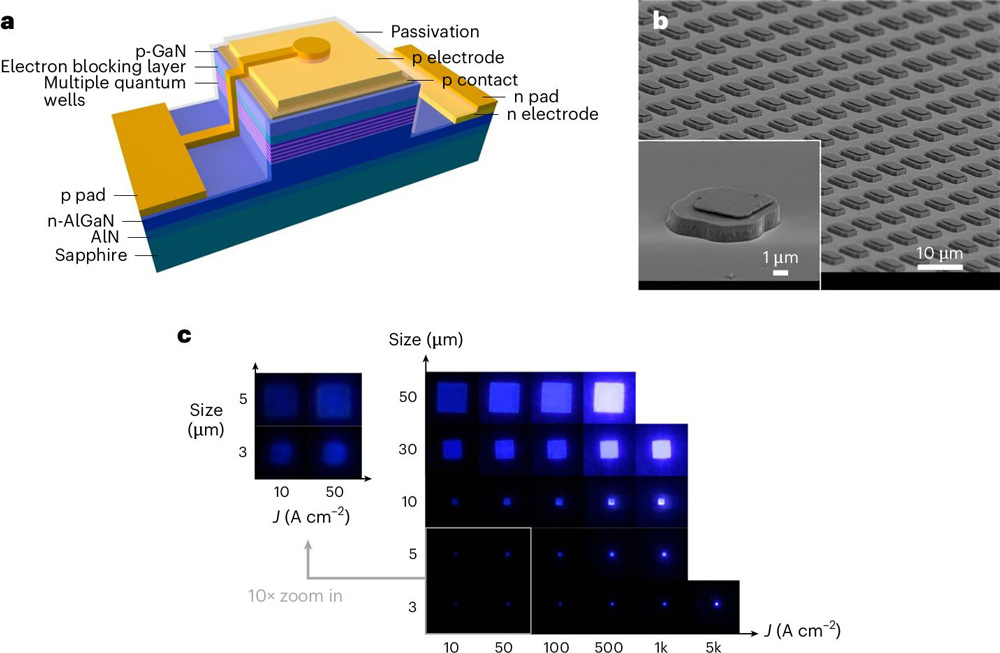
Figure 1: a. Flip-chip UVC micro-LED scheme. b. Scanning electron microscopy morphology of 6μmx6μm UVC micro-LED array, with (inset) stand-alone 5μmx5μm. c. Electroluminescence (EL) micrography of stand-alone devices.
The researchers used commercial 2-inch aluminium gallium nitride (AlGaN) epitaxial wafers to fabricate the UVC LED arrays (Figure 1). The team notes that these wafers were bowed by more than 100μm, creating difficulties: “This pronounced bowing effect poses a major obstacle in achieving large-format UVC micro-LED displays, as it causes substantial alignment gaps during fabrication processes such as electrode patterning, hole etching and flip-chip bonding.”
This bowing is related to strain effects arising from the significant lattice and thermal expansion mismatching between the AlGaN layers and sapphire substrate.
The researchers reduced the impact of the bowing by using small wafer pieces singulated using laser dicing, allowing acceptable accuracy in the array patterning down to 3μm mesa widths.
The top p-contact consisted of ultrathin nickel/gold, which is practically transparent in the UVC wavelength range.
The resulting device demonstrated very low leakage currents under reverse bias, below the 100fA detection limit of the researchers’ measurement equipment. “This can be attributed to the reduced sidewall damage resulting from tetramethylammonium hydroxide (TMAH) treatment and the atomic layer deposition (ALD)-grown sidewall passivation,” the team reports.
Reduced device sizes were found to benefit from higher current density for a given bias, resulting in higher current uniformity across the LED.
The team comments: “The alleviated current-crowding effect and increased surface-to-volume ratios contribute to enhanced heat dissipation in smaller devices, mitigating thermal degradation under high current injection.”
The ideality factor of the devices reduced from 3.9 to 2.8 as the forward bias increased from 3.95V to 4.2V. The high ideality was attributed to non-radiative recombination arising from the unoptimized quality of the epitaxial wafers.
The team suggests that its TMAH and passivation treatments were sufficient to make the sidewalls an almost negligible source of non-radiative recombination centers. However, in the smaller devices down to 3μm there was some evidence that “the passivation and TMAH treatments may not be entirely effective in suppressing non-radiative recombinations originating from defects caused by sidewall damage.”
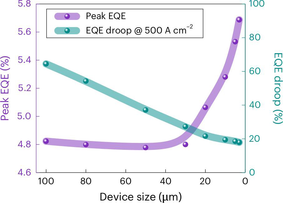
The evidence for this was a pushing of peak external quantum efficiency (Figure 2) to higher current density: from 15A/cm2 to 70A/cm2 as the device size decreases from 100μm to 3μm, respectively. The EQEs were low compared with what can be achieved with blue or green passivated LEDs (an order of magnitude).

Figure 2: Peak EQE and EQE droop ratio, compared with peak value, for each device size (dots) with trend lines.
The team reports: “As the device size decreases, the EQE droop diminishes from 67.5% to 17.9%, indicating that smaller devices offer higher stability of light emission at elevated current densities due to their superior heat dissipation.”
The researchers attribute the increase in EQE for sizes below 30μm to light extraction efficiency (LEE) enhancement along with higher current-spreading uniformity. The researchers explain: “Smaller devices emit light closer to the sidewalls, resulting in more sidewall refraction and consequently higher LEE.”
The peak wavelength of the devices was around 270nm with a full-width at half maximum (FWHM) less than 21nm. The peak wavelength of the 3μm device underwent a 2nm blue-shift at low currents, transitioning to a 1nm red-shift at higher currents above 70A/cm2.
The team comments: “This shift is due to the competition between bandgap shrinkage caused by self-heating and band-filling effects. However, the total spectral shift across all the current densities is only about 2nm, which can be attributed to the enhanced heat transfer path, leading to a slower rise in junction temperature.”
The light output power (LOP) reached 4.5mW at 35mA for the 100μm LEDs, a density of 43.6W/cm2. For the 3μm LEDs the maximum LOP density was 396W/cm2. “Smaller devices, with better current-spreading uniformity and thermal stability, can sustain higher current densities, thereby achieving greater optical power densities,” the team reports, adding: “This may also be due to the waveguiding effect in AlGaN multi-layers, where larger devices experience increased power loss due to a longer optical path from the emissive multiple quantum wells to the air.”
Operating at the maximum power point leads to accelerated aging due to extreme junction temperatures, leading to thermal degradation.
At 100A/cm2, the LOP density for the 3μm device was 25.9W/cm2. The researchers see this as showing “excellent potential as a photolithography light source”.
The researchers managed to increase the size of UVC LED arrays from the 16x16, previously reported in the scientific literature, to 160x90 pixels (2540/inch), based on 6μm devices at 10μm pitch. The arrays were coated with a highly UVC-reflective Al top surface for enhanced rear-side light extraction through the thinned sapphire substrate.
The array achieved an optical output power of 16.6mW at 20A/cm2 current density under 12V forward bias. The peak EQE was 4.1% at 8A/cm2.
The team reports: “The UVC micro-LED display offers an adequate optical power density of up to 1.1W/cm2 for full-screen lighting, surpassing the 25mW/cm2 calibration of the 365nm mercury lamp used in the Karl Suss MA-6 mask aligner to meet the photoresist exposure dose requirements.”
Photolithography capabilities were tested (Figure 3) using a 320x140 UVC array with 9μm pixels at 12μm pitch. The array was flip-chip bonded with indium bumps onto a CMOS driver chip. The photoresist for the test was the i-line sensitive AZ MiR 703 in a proximity patterning setup. The photolithography technique could be used for visible micro-LED displays, for example.

Figure 3: Maskless photolithography images (left) and surface profile (right) revealed on photoresist-coated wafers by UVC micro-LED display photolithography. Exposure was at 80mA for 5s.
The researchers comment: “Although the structural resolution is not as high as that achieved with contact exposure, related lens and focusing systems could significantly improve maskless photolithography. As smaller linewidths down to the pixel size of micro-display chips show great potential, such maskless photolithography systems could provide considerable time and cost savings for the semiconductor industry by eliminating the need for laser-writing masks.”
The researchers hope to overcome the present limitation to 320x140 pixels by enhancing the epitaxial wafer quality and achieving more accurate alignment, paving the way for much-higher-resolution UVC micro-LED displays up to 8K pixels in each dimension, as needed for HD and UHD resolutions.
TrendForce 2024 Micro LED Market Trend and Technology Cost Analysis
Release: 31 May / 30 November 2024
Language: Traditional Chinese / English
Format: PDF
Page: 160-180
TrendForce 2024 Deep UV LED Market Trend and Product Analysis
Release Date: 31 March, 15 September 2024
Languages: Traditional Chinese / English
Format: PDF / EXCEL
Pages: 50-60 / Semi-Annual
|
If you would like to know more details , please contact:
|


 CN
TW
EN


