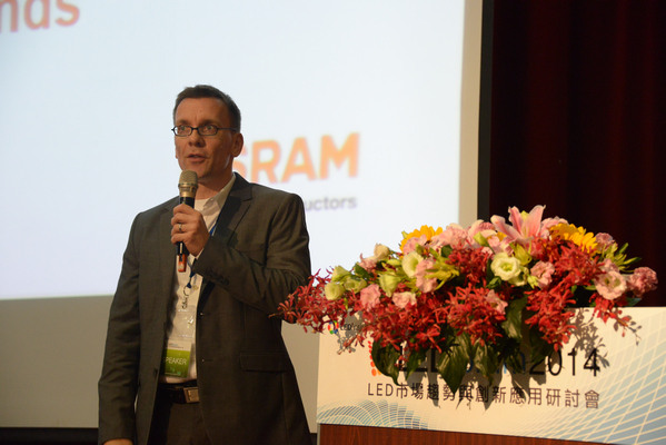
One of Osram’s ongoing projects to overcome LED efficacy limitations is the development of microrod 3D LED technology, said Michael Schmitt, Regional Market Director, Asia-Pacific, Osram Opto Semiconductors.
Many of the current LED designs are 2-dimensional and horizontal, which can restrict light emittance because of its structure, but a 3D LED chip design which incorporates microrods can improve light emission, said Schmitt. Microrods can increase blue and green emission by 5-10% under a 350 mA current, and even boost white LEDs brightness by 10-20%. The technology is also capable of reducing LED droop by just 15% deviation from linear behaviour under of 350 mA to 1W. The forward wattage is also lower for 3D LED from 200 MA to 1W. Microrod materials are mostly InGaN or GaN LED.
 |
|
Michael Schmitt, Regional Market Director, Asia-Pacific, Osram Opto Semiconductors. (LEDinside) |
Usually these microrods have a radius of 1 micrometer, thickness is in the range of 4 micrometers and height is in the range of about 20 micrometers.“It turns out this kind of arrangement is kind of a sweet spot,“ said Schmitt. “If you grow your rods higher of course you can get more area, but at the same time the light has to go out of the chip at a certain point. If you grow your rods higher the more reflection and absorption you get.“
Osram is already mass producing the 3D microrod LED chip, and the actual light distribution of the chips fall in a narrow range of 610 nanometers for mean diameter.
 |
|
Michael Schmitt, Regional Market Director, Asia-Pacific, Osram Opto Semiconductors during the presentation. |
The German manufacturer’s focus on 3D LED chip technology can be explained by four major parameters, which continue to drive LED industry technology developments towards more efficient lights to lower production costs and final retail prices.
The four major parameters used to assess LEDs include luminous efficacy measured by lumens per watt (lm/w), and lumens per dollar (lm/$) which calculates the value of light emission in US dollars. Lumen maintenance or also coined lifetime, and lumen perception, or known as light quality that is commonly represented using CRI. A 20% increase in efficacy is roughly equivalent to 50% reduction in specific luminous costs, said Schmitt.
“You heard in some of the discussions today that we talk about going beyond 200 lm/w, of course this is uneasy, but is possible in LED lights,“ said Schmitt. Current luminance efficacy fall between 100-180 lm/w, while lm/$ is somewhere between 300-1,000. Additionally, lumen maintenance can range between 10,000-50,000 hours, while CRI is in the range of 70-90.
A LED luminaire’s lifetime and maintenance requirements often depends on targeted application market, for instance an industrial LED light or streetlight would be on the higher end for lifetime and maintenance requirements than a indoor luminaire, while light quality is more important in architecture or indoor lighting applications, said Schmitt.
(Author: Judy Lin, Chief Editor, LEDinside)


 CN
TW
EN


