Taiwan’s National Tsing Hua University has developed a method to improve the performance of zinc oxide (ZnO) transparent conductive oxide (TCO) as an electrode for short-wavelength nitride semiconductor light-emitting diodes (LEDs) [Chung-Yen Lee et al, IEEE Electron Device Letters, published online 11 September 2013]. In particular, the method enhances the light output power of an LED emitting 380nm ultraviolet (UV) at 20mA by 166%.
The method uses rapid thermal diffusion to drive zinc and magnesium (Mg) into gallium-doped ZnO (GZO). The MgZnO material system has a range of optical bandgaps from 3.3eV (ZnO) to 7.8eV (MgO), so adding Mg can be expected to increase the transmittance of the material at shorter wavelength.
The extra zinc tackles a problem with ZnO films where the zinc tends to dissociate from the crystal structure at raised temperature, leaving an oxygen-rich residue that reduces the effectiveness of the n-type Ga-doping. In particular, the Ga donor configuration where the dopant substitutes for Zn can be converted to the Ga2O3 dielectric form, degrading the conductance.
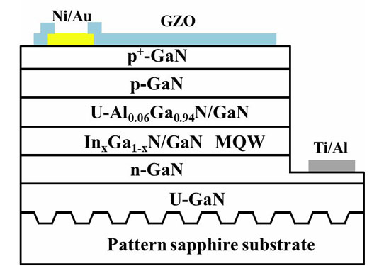
Test LED structures (Figure 1) were grown on patterned sapphire using metal-organic chemical vapor deposition (MOCVD). The undoped GaN buffer was 3μm, the n-GaN contact was 2μm, the multiple quantum well (MQW) active region comprised 9 pairs of 16nm InGaN/GaN layers, and the electron-blocking layer was 6nm of undoped AlGaN. The p-contact/cap consisted of 200nm of GaN (with a hole concentration of about 1017/cm3) and 10nm of GaN (with a higher hole density of 5x10¹⁷/cm3). Violet and ultraviolet emissions were achieved by using InGaN wells with 5% and 6% In fraction, respectively.
 |
|
Figure 1: LED structure for violet and UV LEDs. (photo: Semiconductor Today) |
The LED fabrication consisted of mesa etch and deposition of electrodes. After the structure was annealed at 500°C for 10 minutes, 250nm of GZO was applied as TCO using atomic layer deposition (ALD). The precursors consisted of diethylzinc (DEZn), triethylgallium (TEGa), and water vapor (H2O). The film had a sheet resistance of 15.6Ω/square.
Then rapid thermal diffusion process was used to drive in Mg and Zn into the GZO. The dopant sources were ZnSiOx and MgSiOx spun onto a sapphire wafer that was applied to the top of the LED wafer while thermal diffusion at 400°C was carried out for 5 minutes. The final LEDs were processed by patterning and etching away the excess TCO with hydrochloric acid.
The effect of driving Zn and Mg into the GZO was to increase the transmittance from 83% to 93% at 400nm wavelength. For the even shorter wavelength of 380nm, the GZO as-grown had a transmittance of 80%. Driving in of Zn/Mg improved this to 91%. The enhancement was a reflection of an increase in optical bandgap from 3.64eV as-grown and 3.70eV annealed-only, up to 3.78eV for GZO with driven-in Zn/Mg.
The effect of the Zn/Mg treatment on electroluminescence was to give about 1.4x and 2.5x greater emission at 20mA for 400nm and 380nm LEDs, respectively. The forward voltages at 20mA were, respectively, 3.7V and 4.5V with treatment and 3.9V and 4.2V without.
 |
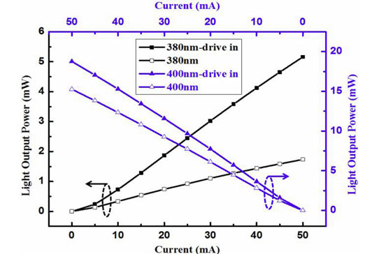
Figure 2: Light output power versus current measured at room temperature for 400nm violet and 380nm UV LEDs with and without Zn and Mg driven-in GZO films. Note: the scale increases from left to right for the 380nm LED and from right to left for the 400nm LED. (photo: Semiconductor Today)
|
Light output power measurements (Figure 2) were carried out on LEDs bonded with aluminum wire and packaged in TO-46S metal cans. The 20mA output powers were 7.7mW (400nm) and 1.9mW (380nm) for the LEDs with Zn/Mg treatment. The respective values for the devices without treatment were 6.1mW and 0.7mW. The enhancements for the Zn/Mg treatment come out at 27% at 400nm and 166% at 380nm.
In addition to the effect from the improved optical transparency, the researchers suggest that there is a boost in light extraction from changes in refractive index.


 CN
TW
EN


