Researchers at the University of Michigan have discovered a way to get 50% more light out of organic light emitting diodes (OLEDs), bringing them one step closer to more widespread adoption as a general lighting source, while increasing their value in displays.
OLED technologies, a nearly US $16 billion market, are already found in more than 750 million smartphone and tablet screens worldwide. The use of organic materials, over inorganic semiconductors used in a traditional LED , makes it possible to have extremely thin, small, and flexible displays – as seen in the Samsung Galaxy or LG OLED TVs, for example. OLED displays also tend to have sharper and more vivid colors, faster response times, truer images from different angles, and require far less power than their LED counterparts.
The appearance of OLED technology in the world of general lighting is steadily growing, and as of 2014 can even be found in lighting fixtures sold at Home Depot. “About 25% of all electricity goes to lighting,” says Stephen Forrest, a prominent leader in the development of OLEDs for commercial use. “And most lighting is terribly inefficient.”
 |
|
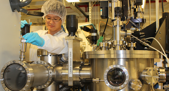
Yue Qu, Electrical Engineering PhD student, in Prof. Stephen Forrest's Lab. (All photos courtesy of University of Michigan) |
Stephen Forrest, Paul Goebel Professor of Engineering, Peter Franken Distinguished University Professor, Professor of Electrical Engineering and Computer Science as well as Physics and Materials Science & Engineering, proposed and developed microlens array technology to double the efficiency of OLED devices back in the early 2000s , reaching 40% in external quantum efficiency (EQE). His team has now increased that relatively 50% further by redirecting light that was previously lost in the OLED light emitting region itself.
More specifically, they've done it in PHOLEDs, which is an OLED that uses a phosphorescent rather than fluorescent material. PHOLEDs have the advantage of being able to reach 100% internal quantum efficiency (IQE), or at least 4 times the potential of a fluorescent OLEDs, as Forrest and his colleagues demonstrated in 1998. PHOLEDs also make stunning displays.
However, while PHOLEDs have 100% IQE, meaning for every electron you put in, you get one photon out, much of the light remains trapped inside the device.
“In conventional PHOLEDs, only 20% of the light emitted from organic molecules makes it out of the devices,” stated Yue Qu, a doctoral student in electrical and computer engineering who helped develop the new technology. “A simple microlens array attached to the glass substrate holding the PHOLEDS outcouple light trapped in the substrates efficiently, doubling the EQE to 40%, but we still want to pull the rest of the light out.”
So where is the rest of the light?
“Much of it is trapped in waveguide modes wiithin the very thin PHOLED light emitting region itself,” explained Prof. Forrest. “For example, the light-emitting molecule, which is randomly oriented, can emit in all directions. If it emits parallel to the glass, it's stuck in the waveguide modes and will never come out. What we need to do is get that light to move perpendicular to the glass.”
“You can be super clever to do this – but the cleverer you are, the more expensive it is. And the more expensive it is, the less interesting it is because while you may be able to get the light out, you can't get the money out” – meaning companies can't get the money out of their investment.
 |
|
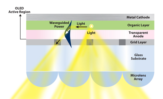
The microlens array, developed by Prof. Forrest's group, increased OLED efficiency from 20% to 40%. The newest addition of a grid layer increases OLED efficiency to 60% by redirecting the horizontal light emitted by the molecule so it can escape the OLED. |
The method the Forrest group came up with is to apply an optical scattering layer of a dielectric grid arrangement beneath the transparent anode layer and above the glass substrate, where there's an index of refraction contrast between the two materials of the grid. That contrast causes the light to be sucked out of the OLED active region and into the substrate, and ultimately, escape the OLED.
“The grid allows 100% of the light in the parallel waveguided power to come out,” said Prof. Forrest. “And any time you pull out an extra photon you win.”
Reducing the energy needed to get the light out of an OLED is extremely valuable for everything from low-power portable electronics to large, higher power screens and lighting. The technique can also be used in photonic integrated circuits.
“To our knowledge it’s the most effective, and cost-effective, method to improve the efficiency of the device, and it doesn’t bother the OLED,” said Forrest “unlike other techniques.”
With this system, the manufacturer of the substrate can build their part of the device completely independently of the OLED manufacturer. The manufacturer of the glass substrate simply needs to coat it with ITO. The process has already been demonstrated in the lab by Yue Qu and former group member Dr. Michael Slootsky (MSE EE ’10; PhD Physics ‘14).
The last challenge is to suppress optical absorption of the metal cathode to improve the EQE even further. Prof. Forrest believes it’ll be possible to reach as high as about 80% EQE with PHOLEDs.
The research is described more fully in the paper, “Enhanced light extraction from organic light-emitting devices using a sub-anode grid,” by Yue Qu, Michael Slootsky, and Stephen Forrest, and published online by Nature Photonics October 12, 2015, in advance of the print publication.
The research was supported in part by Universal Display Corporation, and the work was performed in part at the Lurie Nanofabrication Facility at the University of Michigan.


 CN
TW
EN


