"Great in Optics –Small in Size!" The growing core of the “PolyPhoton- ics” Innovation Initiative will take this motto to the global communica- tions market. The project is part of the “Regional Enterprise Initiative”of the German Federal Ministry of Research. The consortium develops the value chain for the creation of a new technology platform. The Fraunho- fer Heinrich Hertz Institute HHI coordinates the project.
Eleven regional enterprises and three research institutes pool their expertise in PolyPhotonics Berlin. For the first time, the network partners will be able to im- plement comprehensive solutions using optical components made of plastic, which are globally not yet available in this form. The participants in this initiative want to create innovative materials and procedures for the production and as- sembly of photonic multiple-use components.
 |
|
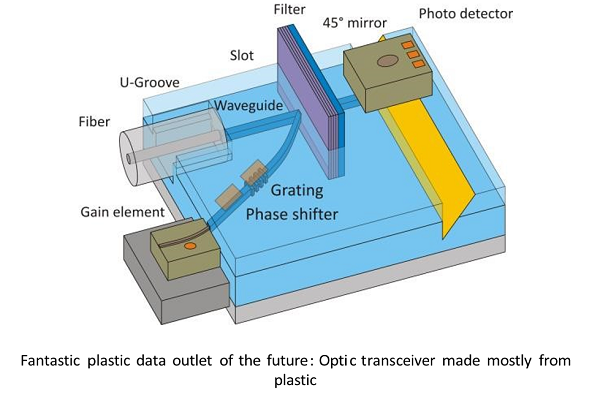
Fantastic plastic data outlet of the future: Optic transceiver made mostly from plastic. (Photo courtesy of Fraunhofer HHI) |
The PolyPhotonics Technology Platform provides a toolbox of hybrid-optical building blocks. Using suitable technologies, members of the initiative put these basic building blocks together to form flexible modules for integration into com- pact functional components of very flexible build (hybrid integration). At the core of the platform is a chip with optical waveguides, which are made of plastic. This chip may feature further passive elements such as optical fibers, thin film filters and micro-optics as well as active elements such as photodiodes or laser chips. In micro technological procedures, the latter components are connected to the waveguide chip. In the group's laboratories, the components are tested and be- come market-ready.
The unique aspect is the use of polymer as material for waveguide boards. This board is needed as component for the socket outlet of the future (see image). This outlet must be ready when data arrive via fiber optic cable. The tiny 1 x 5 Millimeter polymer chips in those sockets will catch a lot of attention outside plug-in connectors as well.
Crispin Zawadzki, Project Manager of the PolyPhotonics Network, explains: "The existing technologies can no longer handle the tidal waves of data streams. In the final analysis, our common research goal is the creation of very small, very potent and very low-cost polymer chips.”


 CN
TW
EN


