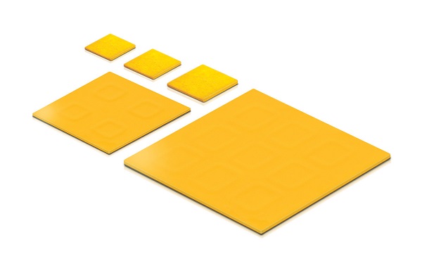
Samsung Electronics Co., Ltd., a world leader in advanced component solutions, today introduced a full line-up of chip-scale LED packages* (CSP), including 0.6W-class and 3W-class packages, CSP arrays, and PoW (Phosphor on Wafer) packages.
 |
Samsung’s CSP technology significantly scales down the size of a conventional LED package by combining advanced flip chip** technology with phosphor coating technology, thereby eliminating any need for metal wires and plastic molds. (Samsung/LEDinside)
|
Samsung’s CSP technology significantly scales down the size of a conventional LED package by combining advanced flip chip** technology with phosphor coating technology, thereby eliminating any need for metal wires and plastic molds. This shift enables more flexible and compact designs when manufacturing LED lighting modules or fixtures, and lowers the production and operational costs of LED lighting systems. Samsung’s CSP products also allow for flexibility in adjusting the size of the light-emitting surface and its associated luminance level, to meet the diverse requirements of a wide variety of lighting applications including bulbs, spot lighting, downlighting and street lighting.
“Our new CSP products overcome what had been significant performance limitations of conventional LED packages. By expanding our CSP line-up, we expect to provide greater value to the LED lighting market, enabling new possibilities in LED lighting and giving our customers greater design flexibility,” said Jacob Tarn, Executive Vice President, LED Business Team, Samsung Electronics. “We are aggressively innovating through the introduction of well-differentiated LED components, while further strengthening our presence in the LED marketplace in terms of technology and cost.”
The new CSP line-up has been fortified with a wide range of operating current options from 0.6W to 3W and even 10W LED packages. The new packages complete Samsung’s CSP technology roadmap, which was announced at LIGHTFAIR International 2015 when the company’s CSP technology commercialization plan was unveiled.
.
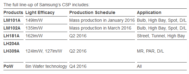
The LM101A and LM102 are Samsung’s new mid-power CSP packages for LED lighting. Based on advanced flip chip technology, the LM101A and LM102A feature ultra-slim form factors and simple package structures that enhance their cost competitiveness. Each offers two voltage options – 3V and 6V, which make the packages applicable to numerous applications including bulb, high bay lighting, downlighting and spot lighting.
Along with enticingly small form factors, the mid-power CSP LED packages also provide wide beam angles, therefore delivering even greater design flexibility. Samsung’s LM101A and LM102A packages are available in full color temperatures with three color rendering index options from CRI 70 to CRI 80 and CRI 90.
The LH181A is a high-power CSP package that features approximately 12 percent higher luminous flux*** at a maximum current of 1.5A, compared to Samsung’s 3W-class ceramic-based high-power LED package. The LH181A offers a high luminous flux, typically at around 162lm/W (@350mA, Ra70, 5000K).
Each LH181A measures 1.91x1.91mm, which is about 30 percent smaller than Samsung’s ceramic-based LED solution. The package’s ultra-small size enables much smaller lighting designs and better lm/$ (lumens per dollar) value that can be especially useful in outdoor and spot lighting applications.
The LH181A provides a wide beam angle of 140 degrees making it also applicable to street lighting by adding a lens as a secondary optic solution.
Samsung’s CSP arrays, the LH204A and the LH309A, are high-power LED solutions with an operating wattage range from 5W to 10W. The LH204A is a 2x2 array of CSP LED chips that delivers 12V at a 5W-class operating wattage, while the LH309A is a 3x3 chip array offering 26V at a 10W-class operating wattage.
The CSP arrays provide high light quality by adhering a single phosphor to the FX (flexible) circuit board on which tiny CSP LED chips with low thermal resistance are arranged. The use of a thin flexible-film FX circuit board accentuates the thin design of the arranged CSP LED chips. The CSP arrays are suitable for spotlighting applications where high light quality is required from a single light source.
Samsung’s Phosphor-on-Wafer (PoW) LED package technology embraces the advantages of CSP LED packaging, while overcoming limitations of cost reduction by upgrading the chip manufacturing process through the use of 8-inch GaN-on-Si wafers instead of 4-inch sapphire wafers. This transition will enable a higher quality CSP LED package by eliminating the chip rearrangement process. The reason for this is that the phosphors can be directly coated on the surface of the GaN-on-Si wafers before being diced, while sapphire wafers have to be cut into chips first and then rearranged to be coated with phosphor.
By simplifying the LED component manufacturing process and improving LED package quality, the PoW LED package technology is expected to contribute significantly to the growth of the LED lighting industry.
Samsung has already applied its PoW technology to 4-inch wafers in flash LED packages for mobile devices since several years ago. Samsung also plans to utilize the PoW technology for its new CSP product line-up for lighting applications by the end of this year.
Samsung will showcase the new CSP products and technologies at the Light + Building 2016 event under the theme “Lighting & Beyond” in Frankfurt, Germany, March 13th – 18th. Visit Booth B04, Hall6.2 to learn more about Samsung’s differentiated LED technologies and innovative component solutions.


