The key for commercializing Micro LED technology is to holistically improve the manufacture process and to achieve cost-effective high volume production of Micro LED displays. Major industry players in the production chain from the LED chip makers, transfer technology developers to panel producers and end products brands have all dedicated themselves to work on solutions for the goal.
Tesoro Scientific, established by Francois J. Henley in 2017, focuses on the enhancement of Micro LED production. Its research paper, titled “Novel In-Process Functional Test Equipment to Enable Micro LED Mass-Production,” was awarded the third place of the Micro LED Technology Research Contest held by LEDinside. In the research, Tesoro introduced an in-process EL (electroluminescent) test approach which is able to examine Micro LED chips before the transfer process and proposed its integrated solution of testing and mass transferring for the next generation Micro LED display production.
LEDinside had a talk with Henley, President and CEO of Tesoro, to understand the innovative approaches of Tesoro and learn how these methods could become effective solutions for Micro LED technology development.

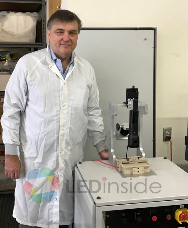
(Francois Henley, CEO, Tesoro; Image: Tesoro)
How in-process functional test can improve Micro LED production yield
In order to achieve cost-effective Micro LED mass production, Tesoro proposes looking into the manufacturing process and identifying critical process steps that can be optimized to improve Micro LED production yield. The article has pointed out that the major processes within the Micro LED manufacturing flow include Micro LED epitaxy substrate formation, donor carrier formation, Micro LED known-good-die (KGD) generation, mass transfer process and Micro LED connections.
With the recognition of these specific processes, Tesoro proposes that combining in-process functional test within certain processes could enhance the overall Micro LED manufacturing yield and therefore help to improve cost and efficiency of Micro LED production. In-process test identifies the defects of Micro LEDs on the epitaxy wafer before moving the LED chips to the donor carrier. Then, prior to the mass transfer process, in-process test can again distinguish the known-good-dies (KGD) to avoid transferring non-functional LEDs to the display substrates. As a result, defective Micro LEDs on wafers and donor carriers would be eliminated before mass transfer, leading to overall yield improvement.
To this end, Tesoro developed a novel EL (electroluminescent) test method that can more accurately identify Micro LED defects compared to the photoluminescence (PL) test. Tesoro also introduced its Beam-Addressed Release (BAR) mass transfer method that incorporate in-process EL test approach to fully optimize the Micro LED manufacturing process.
Tesoro’s non-contact EL (electroluminescent) test approach and Beam-Address Release (BAR) Mass-Transfer Method
Tesoro has noted that EL testing is able to detect the defects that do not show in PL testing, providing detailed information to help reduce the defect rate in further production processes. However, Henley indicated that applying conventional contact EL testing on Micro LED is impossible because the ships are too small. Also, to individually test tens of millions of Micro LED chips within an EPI or carrier substrate is not a feasible option. To address these challenges, Tesoro’s non-contact EL test approach was developed to efficiently sort and bin functional and unfunctional LEDs before mass-transfer.

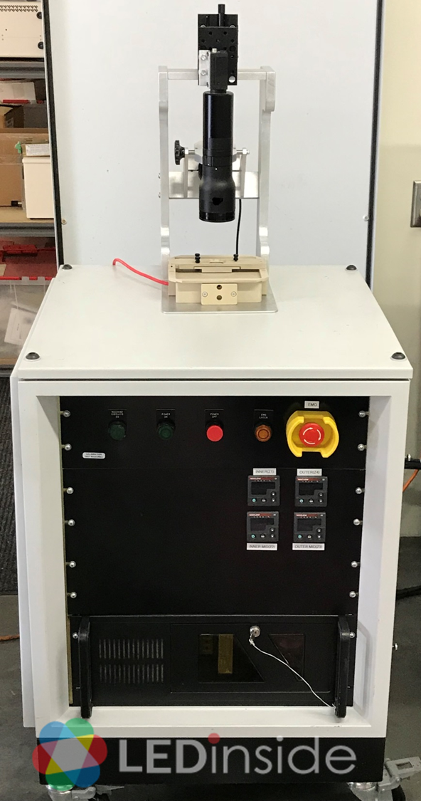
(Tesoro EL Testing )
The non-contact EL test approach developed by Tesoro use structures and integrated layers present on carrier substrates to inject current and measure the LED device’s electro-optic response. The results are processed to yield a KGD map of Micro LED functionality that can drive a high-yield mass transfer process.
Micro LED mass-assembly with Tesoro’s Beam-Address Release (BAR) method is uniquely designed to use the in-process test KGD information using a proprietary method and architecture called “Smart-Assembly”. Henley explained that an ablation layer for Micro LED mass transfer can also be embedded as an internal layer within the carrier substrate. The structure allows individual Micro LED chips to be optically selected and released onto a target substrate with high speed.

(Image: Tesoro)
By combining its non-contact EL test technology with its compatible BAR mass transferring “Smart-Assembly” method, Teroso aims to develop a solution for cost-effective high-volume Micro LED production and has developed an equipment roadmap to address R&D and manufacturing requirements.
Development progress and potential collaboration of Tesoro
According to Henley, Tesoro will build the R&D tool for the EL testing method and BAR mass transferring within 12 to 18 months. As for the equipment targeting consumer Micro LED products, Henley said it would be at least two years away. Meanwhile, as Tesoro has begun partnerships with other LED makers or panel producers, demonstration using these new test and mass-transfer methods might be disclosed by its partners soon.
For further progress of the technology, Henley noted that Tesoro has been in the process of raising its Series A capital funding. In addition, several industry players including LED manufacturers and panel makers have connected with Tesoro for potential collaboration in developing Micro LED display manufacturing processes using Tesoro equipment. Henley addressed that end product producers have also shown their interests in the technology for customized adoption. A mobile phone maker has contacted Tesoro to learn the possibility of adopting the technology into portable devices while some automotive display producers also hope to incorporate Tesoro’s solutions for deploying Micro LED in automotive products and applications.
Comments from the Judges
Judges at the Consortium for Intelligent Micro-assembly system (CIMS) at ITRI and National Chiao Tung University acknowledged how EL testing could become a solution for improving Micro LED production yield and showed interests in learning how the concept could be realized.
See full paper: Novel In-Process Functional Test Equipment to Enable Micro LED Mass-Production


