Why is it Important
Augmented Reality (AR) is thought by many, including many of the leading CEOs in Silicon Valley, to be the “next big thing,” ultimately displacing our smartphones with stylish, interactive glasses that communicate with the digital world, in part by superimposing virtual images on the wearer’s field of view. Huge investment is pursuing this vision, much of it focused on micro-displays and sophisticated optics for overlaying images onto a wearer’s view. But just as promising is the idea of scanning such images directly into the human eye. Needed are very low power lasers or laser arrays in RGB or more colors that can be packaged in very small, discreet form factors suitable for integration into attractive, fashionable eyewear. Such lasers do not yet exist, but a technology that meets the challenge is in development, which can also lever the existing manufacturing infrastructure for LEDs. It can also address many other applications in emerging bio-tech and even in SSL markets for highly directional lighting.
Retinal laser scanning technologies are not new. The technology stems from the 80’s, originally developed as automated laser ophthalmoscopes; the Air Force also developed helmet mounted technology to find where a pilot was looking and display images directly onto the retina, so-called Virtual Retinal Displays (VRD). Commercially, analogs of the general concept, using laser scanning approaches for Heads-Up-Displays (HUD) displays and pico-projectors have been around a while: Microvision (MVIS) has long been preaching the virtues of its PicoP technology, TI, Compound Photonics, and many others have long been working on pico-projection, while Intel (INTC) had recently acquired IP and several Swiss start-ups (Composyt, Lemoptix) targeting the AR space. While many applications that are tethered to power such as cockpit HUDs or helmet AR, ophthalmology instruments, etc., may not be very sensitive to size and power constraints, the scale and power needs of current devices are generally much too large for many applications, particularly for any vision of discreet, stylish, and highly mobile future AR.
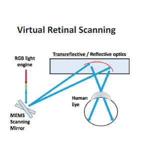
For VRD, cutting edge research has been focused on scanning MEMS mirrors and a variety of novel transreflective optics and architectures (that are mostly transparent, but reflect select wavelengths) to scan a laser beam directly onto the retina to form an image. For example, advances in optical architectures allow a more expanded “pupil box” than was possible in the past; the human eye is rarely static and a wider pupil box leads to a more desirable and natural user experience.
 |
|
(Image: VerLASE) |
To allow creation of multiple spatial frames, these advanced optics often require multiple and distinct sets of RGB colors, with each set of R,G,B colors separated from each other by 10’s of nm. The burden on the laser sources, in terms of size, power, multiple colors and spectral separation, let alone cost is significant.
Whatever the specific scanning technology used, what are inevitably needed are low power, low cost laser arrays across the visible, with optimized RGB wavelengths per node as required.
Thus far, laser diodes (LDs) have largely been practical in blue/violet wavelengths, based on similar InGaN technology as the LEDs used in SSL. They are used in a variety of applications, and increasingly in projectors and in automotive headlights (using blue laser pumped phosphors). Some LDs and low-density LD arrays have also been available in green (520 nm), but power and efficiency drops off dramatically with longer wavelength. In general, LDs have thus far tended to be discrete devices, available only in very limited colors. There are no good, direct-emitting LD solutions in a broad region of the visible, loosely in the range of 535 nm (Green) to 620 nm (Red). Moreover, they tend to be edge emitters with larger spectral bandwidths than cannot easily be used with the advanced optics being developed. The current state-of-art for visible LD technology can be categorized as follows:
-
Direct emission, edge-emitting LDs based on III-V Nitrides in the range of approximately 380 to 520 nm, with efficiencies from 45% in the blue/violet, deteriorating rapidly with wavelength to <<15 % in the Green. Due to entrenched IP positions and high barriers to entry, the market is controlled by Nichia and Osram, and to some negligible market share by Soraa Laser Diode.
-
Second Harmonic Generation utilizing NIR pump sources, which include variations such as Diode pumped doubled solid-state (DPSS), Semiconductor diode doubled laser, Diode pumped semiconductor diode doubled laser, and optically pumped VECSEL (Vertical External Cavity Surface Emitting Laser). Barriers to entry are lower, and there are many more players, but the resulting light is not particularly suitable for some key applications due to multiple reasons (low efficiency, temperature stability, high coherence / speckle, form factor, discrete wavelengths, … etc.)
-
Due to significant material / process challenges with III-V Nitrides, there are no electrically pumped VCSELs (Vertical Cavity Surface Emitting Lasers) commercially available today in the visible range (but they are ubiquitous in the NIR, by some accounts accounting for the vast majority of LDs used in datacomm applications).
While Optically Pumped Semiconductor, Vertical Cavity Surface Emitting Lasers (OPS-VCSELs) are known, they suffer from many shortcomings. The Quantum Wells (QWs) for the gain section in such devices need to be thin enough for the right wavelengths, but while absorption coefficients for the direct bandgap semiconductors that form the QWs are higher for a given thickness than that for typical solid-state laser materials, the corresponding absorption is too low in the thin QW layers required. Consequently OPS-VCSELs in the prior art have had to use dual pass, and other complicated multi-pass architectures to absorb enough input pump light.
One other solution for absorbing more light has been to use an external cavity, one example depicted in the adjacent figure. Such an OPS-VECSEL scheme effectively combines two resonators, one to satisfy resonance conditions for the input pump for increased absorption, and the other for the desired output emission. The most commercially successful example of this approach may perhaps be the Optically Pumped Semiconductor Laser (OPSL) from Coherent, but a robust, monolithic, integrated solution in the form of an OPS-VCSEL has not yet been found.
A simple, low cost technology that can efficiently downconvert laser light from widely available, reasonably inexpensive blue/violet LDs or LD arrays (e.g. from Nichia or Osram) to any desired color in the visible while maintaining stimulated emission would be immensely valuable not only for direct scanning into the eye in AR applications, but in a wide range of applications where visible laser sources are needed.
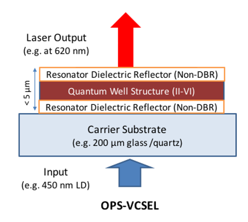
Where most current R&D on LDs in the visible has focused on electrically driven devices, VerLASE has developed an optically driven approach more efficient than any known electrically driven technology for wavelengths above 520 nm or so. It addresses the core challenges with a novel, highly manufacturable architecture forming a monolithic (not external cavity) OPS-VCSEL that solves the prior art issues.
A variation of its Chromover™ technology developed for color conversion in emerging microLED micro-displays, it consists of a gain media comprised of direct bandgap semiconductor QWs bounded on either side by VerLASE’s patented coatings to form a novel resonator. These QWs can be of either II-VI materials, or depending on target wavelength, similar III-V Nitride chemistry as the pump LDs. The structure can be pumped by low cost, widely available, III-V Nitride LDs (for example, at 405-450 nm) or by a controlled array of such LDs, very efficiently emitting downconverted laser light.
The core IP involves a novel resonator satisfying conditions of resonance for both the input pump and the output emission at the same spatial location. Light absorption with QWs at this location is dramatically increased to over 98% with the fewest number of QWs, increasing efficiency and reducing thermal management issues. It enables practical use of a broader range of direct bandgap semiconductor materials, and is not limited to the visible. With material sets photoluminescing (PL) in other spectral regions, the technology can also be extended into the UV and IR ranges, depending on available pump sources.
 |
|
(Image: VerLASE) |
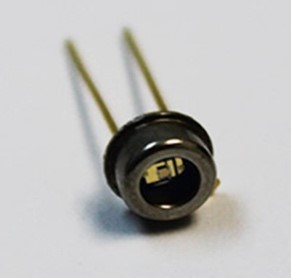
The monolithic structure presents as a tiny chip that can also be co-packaged with the laser pump source in a compact package as an individual downconverted LD, or it can also be designed for multiple colors on a single chip overlaying a LD array to form a RGB laser source in an ultra-compact form.
 |
|
(Image: VerLASE) |
Advantages
I. The output Center Wavelengths (CWLs), whether in an RGB array or as a single OPS-VCSEL, can be designed to be anywhere needed between 480 – 625 nm, depending on the choice of QW semiconductor material and pump wavelength. Multiple wavelengths will be needed in next gen AR applications, and ability to select optimal colors allows better matching to the photopic sensitivity of the human eye; less power is needed for optimal colors to be perceived as equally bright.
II. The efficiencies of sophisticated new optics used to help scan images into the eye are sensitive to input angles and spectra; some control of output beam shape and spectral characteristics is imperative. Similarly, the manufacturing tolerances of next generation optics can be reduced with more tolerant laser sources. OPS-VCSELs also have circular, rather than elliptical output beams.
III. A thin, vertical emitting structure such as the proposed OPS-VCSEL has much greater output CWL temperature stability than the longer edge-emitting structure.
IV. Output spectral bandwidth can be tailored to a degree to suit specific applications, for example, from < 0.5 nm to > 3 nm.
V. Multiple colors can be designed in the same chip, and pixelated to suit, for LD arrays /RGB laser sources, or wavelength diversity in systems /applications requiring some degree of speckle control.
VI. The output resonance conditions are independent of the input; the quality of the input laser becomes less important. The CWL /FWHM and spectral drift of the pump laser source can vary widely, since the resonator can accommodate a wide input spectral range.
VII. Similarly, the input pump can be multi-mode and/or designed for off normal incidence, allowing power scaling with multiple pumps for certain applications: the output can then be single mode and high quality at a down-converted wavelength of choice (if within the PL range of the QWs).
VIII. Direct bandgap semiconductor QWs allow fast switching /modulation (but depend on modulating or switching of the input laser pump source).
IX. The OPS-VCSEL is scalable in power with pump spot size for low and medium powers (<1 W) (compared to electrically pumped VCSELs where output power is limited by physical size).
X. Unlike traditional electrically driven VCSELs, the structure of the proposed OPS-VCSELs is much simpler without charge injection and electrical transport layers: monolithic, efficient and compact, it can be co-packaged with the laser pump source in transmissive or reflective layouts.
In sum, the proposed OPS-VCSELs bring an array of unique features to the creation of higher efficiency laser diodes in the visible and beyond.
Manufacturability
Key in the OPS-VCSEL architecture and manufacturing devices is growing the semiconductor layers that comprise the QWs; the resonator itself is materials agnostic with respect to the QWs and can be designed for different input/output wavelengths and wavelength regions from UV to NIR. In the visible range, VerLASE has been using direct bandgap II-VI materials made by industry standard, molecular beam epitaxy (MBE) for high layer accuracy and low defect concentration.
However, III-V Nitride materials such as InGaN broadly used for LEDs can also be used. By increasing Indium content in InGaN QWs, their PL range can be pushed toward 600 nm, and since the QWs are a passive, optically pumped layer, with no charge injection layers or current flow, they can be readily manufactured. Widely available metal-organic chemical vapor deposition (MOCVD) with high layer accuracy and low defect concentration can be used; the choice of manufacturing methods driven by the materials involved, in turn driven by the desired spectral range, convenience and cost.
The principal manufacturing steps have been proven in the development of a basic, proof-of-principle prototype using II-VI materials and manufacturing costs extensively modeled; however, better prototypes are needed, especially for InGaN based versions. In addition, substantial computer modeling has been done by an independent, highly regarded source to validate the overall concepts.
The proposed technology using InGaN-based QWs can lever proven, installed capacity for InGaN-based LED manufacturing (some would say substantial overcapacity, especially in China with huge MOCVD equipment purchases by Chinese LED manufacturers in recent years). There are many MOCVD foundries around for a fully outsourced model with lower net costs. Moreover, using the same proven InGaN materials as in LEDs may make a new technology more acceptable in the market.
Conversely, it offers LED manufacturers with III-V nitride capability a channel to enter the market for visible lasers by manufacturing OPS-VCSELs, a much higher value, IP protected product than LEDs. VerLASE seeks partners interested in co-developing, licensing, or otherwise helping the Company exploit the technology for AR applications and in multiple other laser markets.
The technology scales in power, wavelength and allows multiple wavelengths on the same chip in pixelated configurations for arrays, depending on the underlying pump source. More sophisticated variants can allow for multiple outputs per single input, and either simulated or spontaneous emission, enabling new markets in lasers (tunable visible lasers), directional lighting (SSL), and others … Applications that particularly lend themselves to this technology include:
-
Automotive Heads Up Displays (HUDs) (Low Output powers, Speckle mitigation);
-
A wide variety of life sciences, bio-med diagnostic and instrument apps (e.g. fluorescence, plate readers, flow cytometers, spectroscopy, and bio-chip /lab-on-chip type applications);
-
Emerging Smartphone integrated medical diagnostic solutions (personalized medicine);
-
Many observers, among which Nobel Laureate Shuji Nakamura, believe LDs rather than LEDs are the future in SSL; a robust downconverting mechanism yielding RGB for easy mixing is key.
And myriad other laser applications where this technology fits well.
Summary
For AR applications using VRD, efficient low power lasers or laser arrays in RGB and multiple colors are needed that can be packaged in very small, discreet form factors suitable for integration into attractive, fashionable eyewear; however, LDs and LD arrays have largely been limited to blue/violet wavelengths and have thus far tended to be discrete devices. There are no good, direct-emitting LD solutions much beyond 520 nm, and no direct LDs in the range of 535 nm (Green) to 620 nm (Red). Moreover, what LDs there are tend to be edge emitters.
VerLASE has developed an optically driven OPS-VCSEL technology that very efficiently downconverts laser light from low cost, widely available and relatively efficient (e.g. from Osram or Nichia) III-V Nitride pump LDs, or by a controlled array of such LDs, operating at 405-450 nm. It combines a unique resonator with direct bandgap semiconductor QWs where the resonance conditions for both the input pump and the output emission are met at the same spatial location, dramatically increasing absorption to over 98%, increasing efficiency and reducing thermal management issues.
The monolithic structure presents as a tiny chip that can also be co-packaged with the laser pump source in a compact package as an individual downconverted LD, or designed for multiple colors on a single chip overlaying a LD array to form a RGB laser source in an ultra-compact form.
The technology is materials agnostic with respect to the QWs. In the visible, direct bandgap II-VI materials as well as III-V materials such as InGaN broadly used for LEDs can be used, and with material sets photoluminescing in other spectral regions, the technology can even be extended into the UV and IR ranges. The principal manufacturing steps have been proven in developing a basic II-VI prototype, with extensive computer modeling by a highly regarded independent source to validate the overall concept.
If InGaN QWs, the technology can also lever many MOCVD foundries for a fully outsourced model with lower net costs, or lever the huge capacity put in place for LED manufacturing in recent years, especially in China. Conversely, the OPS-VCSELs offer LED manufacturers a path to the market for visible lasers with a much higher value, IP protected product than LEDs.
In sum, the technology addresses the core challenges with a novel, highly manufacturable architecture forming a monolithic OPS-VCSEL that solves the prior art issues. VerLASE seeks partners interested in co-developing, licensing, or otherwise helping the Company exploit the technology for AR applications and in multiple other laser markets.


 CN
TW
EN

