Tsinghua University and Beijing National Laboratory for Condensed Matter Physics in China have reported on the use of freestanding gallium nitride substrates (FGS) for red indium gallium nitride (InGaN) micro-light-emitting diodes (LEDs) in terms of efficiency and uniformity across arrays of devices [Luming Yu et al, Appl. Phys. Lett., v123, p232106, 2023]. The researchers claim that InGaN red micro-LEDs with etching-defined mesa size <5μm have not previously been reported.
Although it is difficult to achieve high efficiency using indium gallium nitride (InGaN) in the red section of the visible light spectrum, there has been much effort in recent times, particularly for micron-sized devices as used in arrays for micro-displays aimed at augmented-reality and virtual-reality (AR/VR) applications, such as head-up displays (HUDs) in military aircraft pilot helmets.
The advantages of InGaN over the more traditional red LED materials, such as aluminium indium gallium phosphide (AlInGaP), include easier integration with green and blue InGaN LEDs, and better scaling to smaller device sizes due to less migration of carriers to sidewall defects, where recombination tends to be non-radiative.
Device materials were grown on FGS from Nanowin and reference material was grown on patterned sapphire substrate (PSS) by metal-organic vapor phase epitaxy (Figure 1). The n-GaN buffer/contact was 2μm thick on the FGS sample and 5μm on PSS.
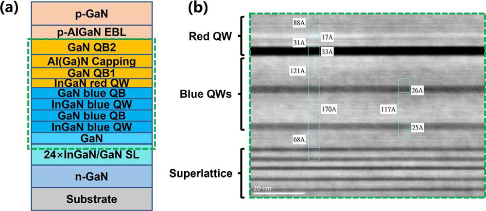
Figure 1: (a) Schematic epitaxial structure. (b) Enlarged transmission electron microscope (TEM) image of green box in (a).
The structure included pre-strain layers consisting of a 24-period InGaN/GaN superlattice (SL) and two blue InGaN quantum wells (QWs), separated by GaN quantum barriers (QBs). The red-emitting part of the structure consisted of a single QW and a three-stage structure of two GaN barrier and aluminium gallium nitride (AlGaN) capping layers. Hole injection was provided by p-doped AlGaN electron-blocking layer (EBL) and GaN contact layers.
Single devices and arrays of red InGaN LEDs were fabricated using direct-write electron-beam lithography patterning, inductively coupled plasma etch, and plasma-enhanced chemical vapor deposition (PECVD) of silicon nitride passivation. The devices were not intentionally optimized.
Electrical testing was on-wafer using contact probes. Light was collected through the substrate in a 60° half-angle cone.
Reverse-current leakage measurements indicated significant sidewall damage of the devices, which dominates performance at smaller device sizes. The reverse leakage at −5V increased from 10−3 to 1A/ cm2 as the devices reduced in size from 20μm to 1μm. With 5A/ cm2 forward current injection, the peak wavelength was 631nm on FGS (sample A) and 603nm on PSS (sample B). Both spectra showed a full-width at half maximum (FWHM) of about 60nm.
The researchers comment: “The longer wavelength of sample A is attributed to the larger lattice constant of FGS, which is conducive to the incorporation of indium.”
Emission from the blue QWs (~460nm) was approximately more than a factor of 10 less intense. Some even shorter wavelength radiation ~400nm was attributed to electrons overcoming the EBL and reaching the p-GaN contact layer before recombining.
The peak external quantum efficiency (EQE), achieved at 50A/ cm2, on sample A was 1.73% for a 20μm device and 0.86% for a 1μm device. The peak wavelength was of order 614nm. The peak EQEs for sample B were 1.05–1.62% at the same injection, but the wavelength had blue-shifted to 590nm. In general, the LEDs based on sample B (PSS) had peak wavelengths some 40nm shorter than those based on sample A (FGS).
On the basis of ray-tracing simulations, the researchers estimate the total peak EQE of the 1μm LEDs to be 1.95% on sample A and 2.78% on sample B. The corresponding internal quantum efficiencies (IQEs) were estimated to be 7.09% and 6.00%.
In 10x10 array formats, the 1μm LEDs from sample A showed a relative brightness variance of 0.27 at 10A/cm2 injection, and 0.13 at 100A/ cm2 (Figure 2). The respective values on sample B were 0.79 and 0.29.
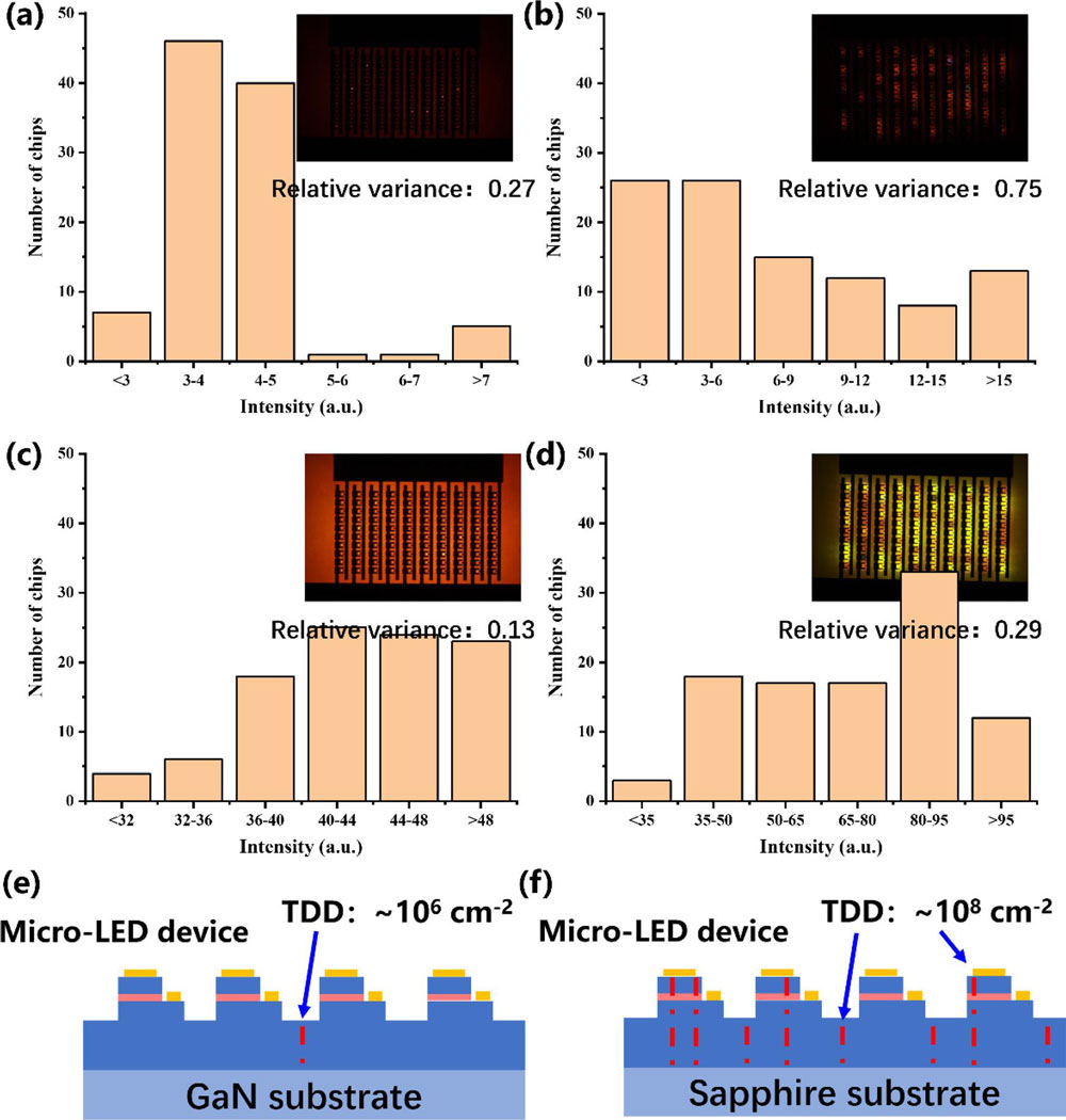
Figure 2: (a)–(d) The brightness distribution of 10x10 arrays of 1μm micro-LEDs under different conditions. (a) Sample A and (b) sample B at 10A/ cm2. (c) Sample A and (d) sample B at 100A/ cm2. Insets: electroluminescence (EL) photos at corresponding current density. (e) and (f) Schematic diagrams of micro-LED chips on different substrates according to defect densities.
The researchers attribute the higher variances on B to its higher threading dislocation density: estimated at 2.29x10⁸/ cm2, according to x-ray diffraction analysis, compared with the 3.5x10⁵/ cm2 specification of Nanowin’s FGS. The researchers admit that the TDD after epitaxy will likely be higher than the spec, but it is difficult to estimate using x-ray analysis when the FWHM of rocking curves is no longer dominated by the impact of threading dislocations on the uniformity of the crystal structure.
At a TDD of order 108/ cm2 there would be on average one dislocation per 1μm LED. However, random fluctuations will lead to some having no dislocation and others two dislocations (Poisson distributed?). Such variations lead to a higher level of brightness non-uniformity for sample B, compared with the lower-TDD sample A.
TrendForce 2023 Micro LED Market Trend and Technology Cost Analysis
Release Date: 31 May / 30 November 2023
Language: Traditional Chinese / English
Format: PDF
Page: 160 / Year
If you would like to know more details , please contact: