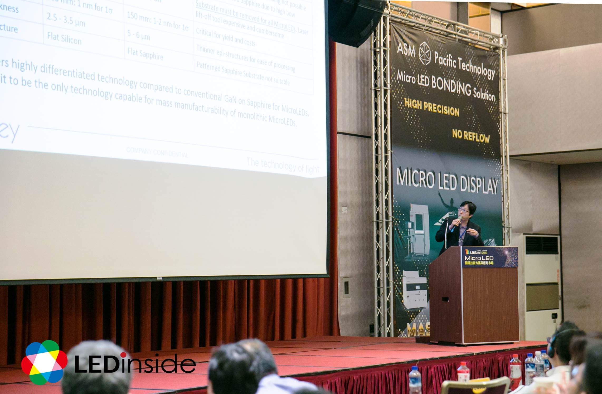
Micro LED technology breakthroughs continue to progress in order to tackle challenges occurred in different manufacture process. At Micro LEDforum 2019, professionals in industry introduced their progresses of various technologies for a wide range of Micro LED applications.

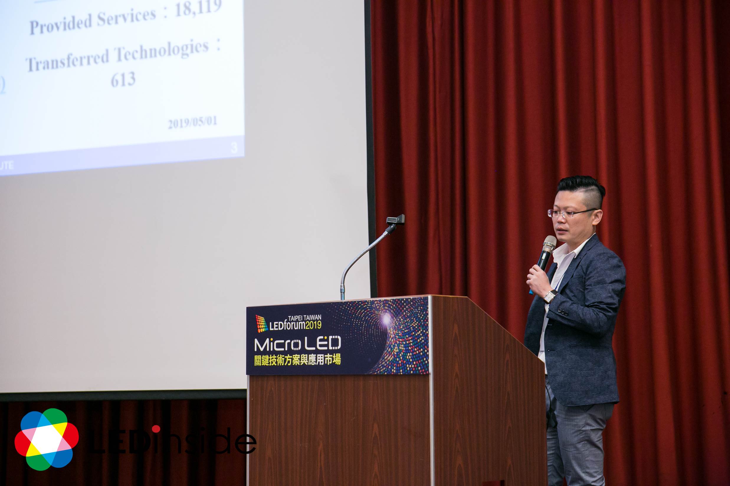
Yen-Hsiang Fang at Consortium for Intelligent Micro –assembly System (CIMS) of Taiwan’s Industrial Technology Research Institute (ITRI) presented the developments of the organization. ITRI began to build up its full color Micro LED display technology since 2014 and has developed Micro LED chips in different structures. With LED chips without sapphire, ITRI has achieved Micro LED chips sized only 5*5 μm with an efficiency of five percent (EQE).

((Yen-Hsiang Fang, Deputy Division Director / CIMS, ITRI))
Based on different kinds of Micro LEDs, ITRI also explores suitable solutions for different applications. For Micro LED RGB signage, ITRI is able to reach a 99 percent yield after transfer and 100 percent yield after repair. The signage module was demonstrated at SID 2019. ITRI is also working on Micro LED-based gaming displays and AR displays as well as sensor integrated Micro LED applications such as transparent displays that can be deployed in wearables and automotive applications.
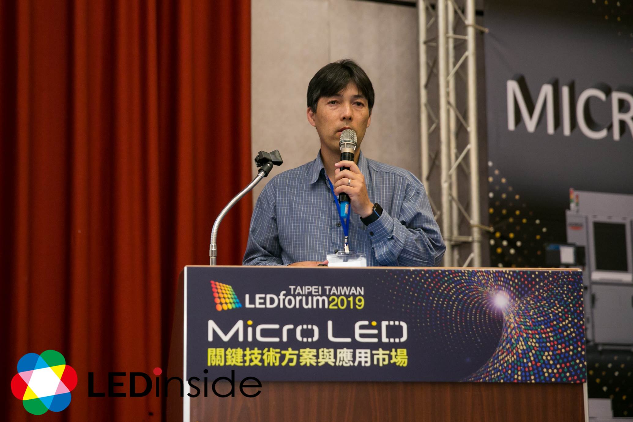
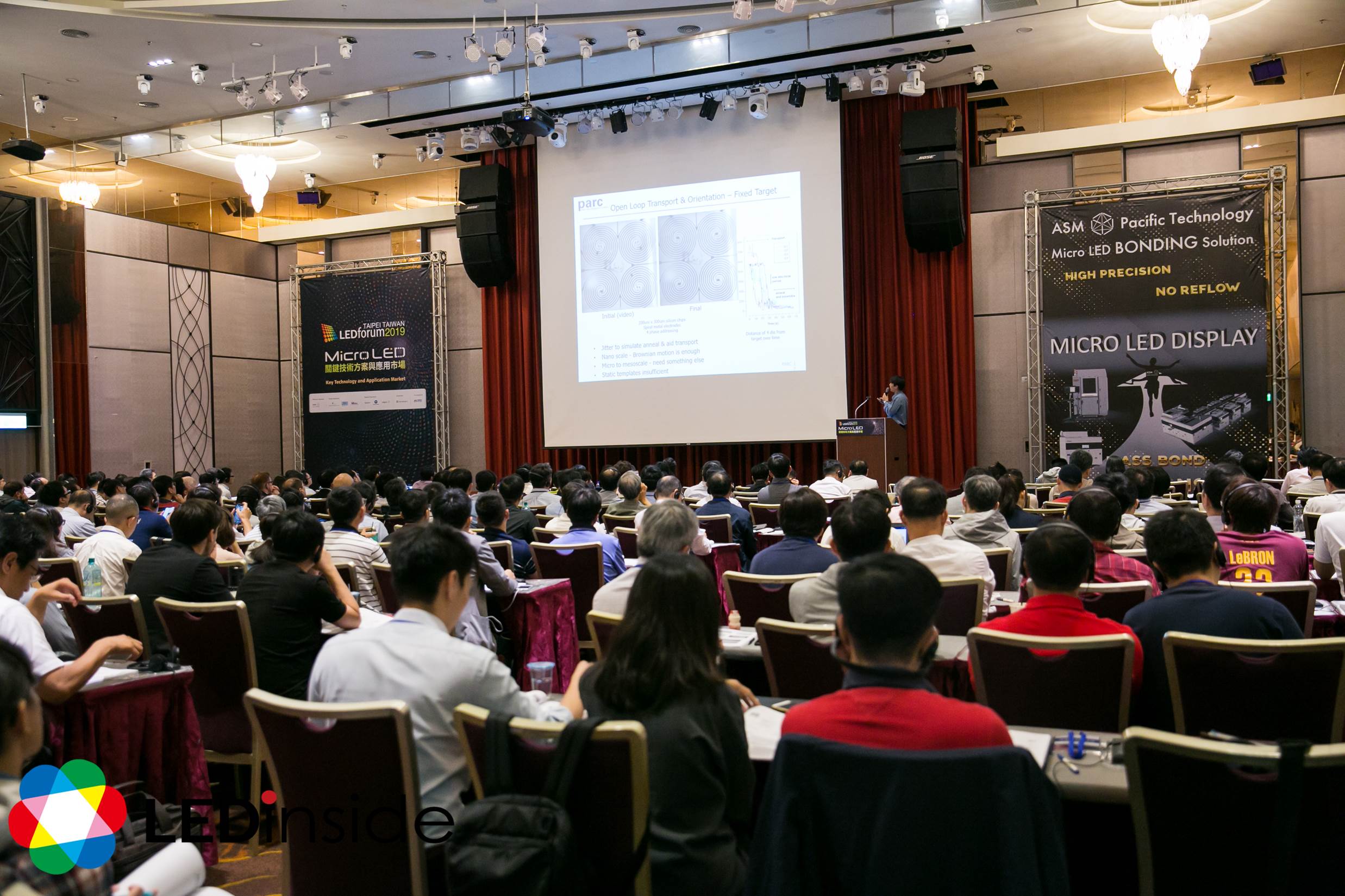
Research company PARC illustrated how its “Micro Assembler Printer” technology can be applied in Micro LED display development. Eugene Chow, Principal scientist and manager of the micro systems research group at PARC noted that its technology integrated nanotechnology and digital printing. With the method, chiplets in solution can be sorted and assembled in parallel with a deterministic and programmable electrostatic assembly process. The assembled Micro LED array can then be transferred to final substrate.

(Eugene Chow, Principal scientist and manager of the micro systems research group at PARC)
The approach enables different sized Micro LED chips and other materials such as micro sensors to be transferred and assembled at once in various modes according to the requirement of different applications. Chow showed several video clips to demonstrate that three types of heterogeneous chips can be assembled at same time in short. PARC has achieved assembly with 10 μm*15μm sized chips and 200μm*300μm sized chips with a prototype system, which has the potential to scale to high throughput and large areas like fluidic assembly.

Plessey shared the features of GaN-on-Si Micro LED, underlining that compared to GaN on sapphire wafers, GaN on Si wafers can be thinner and the substrate can be removed more easily which are crucial for Micro LED manufacture. Moreover, its efficiency performance is better even when chips are smaller.

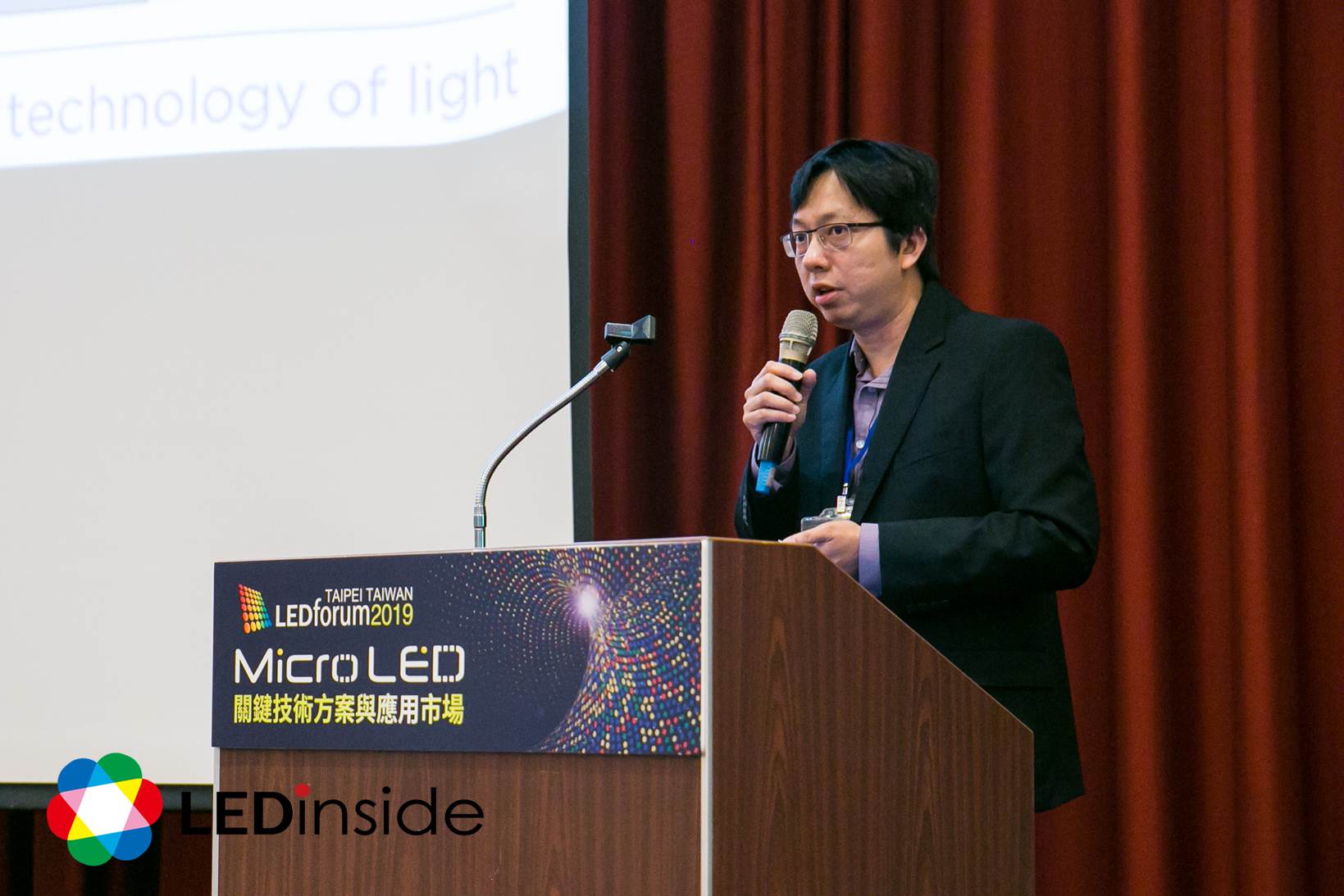
(Dr. WeiSin Tan, Director of Epitaxy and Advanced Product Development, Plessey)

Plessey uses quantum dots (QD) to achieve full color combining blue source with red and green QDs. However, if Micro LED pixels are smaller than 5μm, current QD materials will not be able to apply. During the presentation, Dr. WeiSin Tan, Director of Epitaxy and Advanced Product Development, also shared the latest progress of Plessey. Its 0.7-inch Micro LED display can achieve a resolution of 1080*1920 with a pixel pitch of only 8μm.


 CN
TW
EN

