TrendForce hosted the Micro
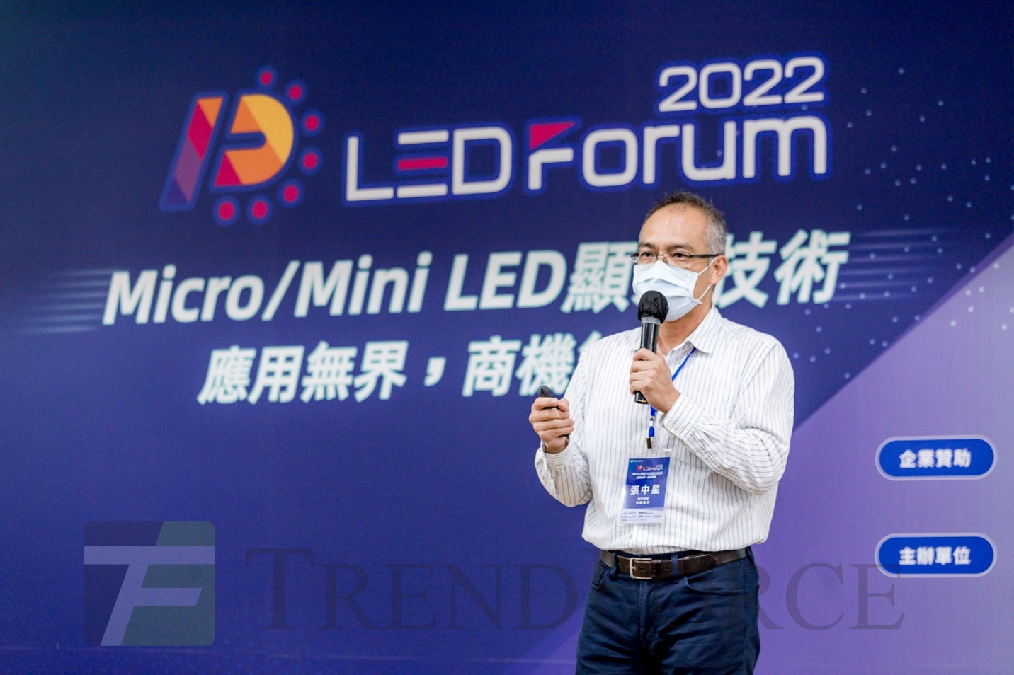
LED Forum 2022 seminar at the NTUH International Convention Center on September 13th. Large display, among numerous Micro LED display applications, is the most anticipated product for the current stage, which is why experts from the Micro LED industry were invited to respectively interpret the technological development and solutions for large Micro LED displays, including the increase of wavelength uniformity in chips, applicability of laser mass transfer and stamp mass transfer, as well as the selection of active glass backplanes and passive backplanes. The guidance of the speakers had seemingly established a consistent target for the Micro LED industry, which is rapid cost reduction that will accelerate the mass production of Micro LED products. This coverage on the seminar will provide snippets pertaining to the technological development and applications of large Micro LED displays and Mini LED backplanes.
From Mini LED to Micro LED; an LED Solution that Can be Mass Produced
Speaker: Tseng Chun-ren
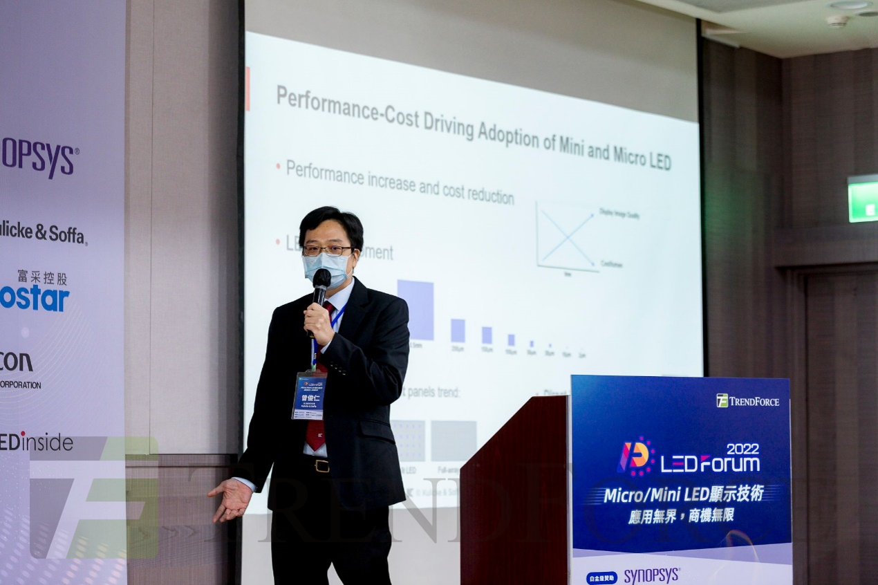
Senior Technical Manager / Kulicke & Soffa
K&S speaker Tseng Chun-ren commented that the company has been long cultivated in the development of Mini LED backlight module transfer, and uses Pixalux for the mass production of Mini LED, which mechanically transfers Mini LED onto backplanes at a capacity of roughly 50Hz. In order to respond to the trend of Micro LED, K&S has developed Luminex’s laser mass transfer equipment that transfers Micro LED onto backplanes, with an amplification in capacity to 100-10,000Hz. This particular laser transfer largely differentiates from other methods in the industry, and the biggest difference is that the DRL is hit with laser pulse through a transparent substrate, where bubbles would then form within the DRL due to thermal reaction, and Micro LED chips are extruded and released before they are fallen onto the DCM.

Display Solutions from Passive to Active Drivers
Speaker: Doctor Hsu Ming-chi
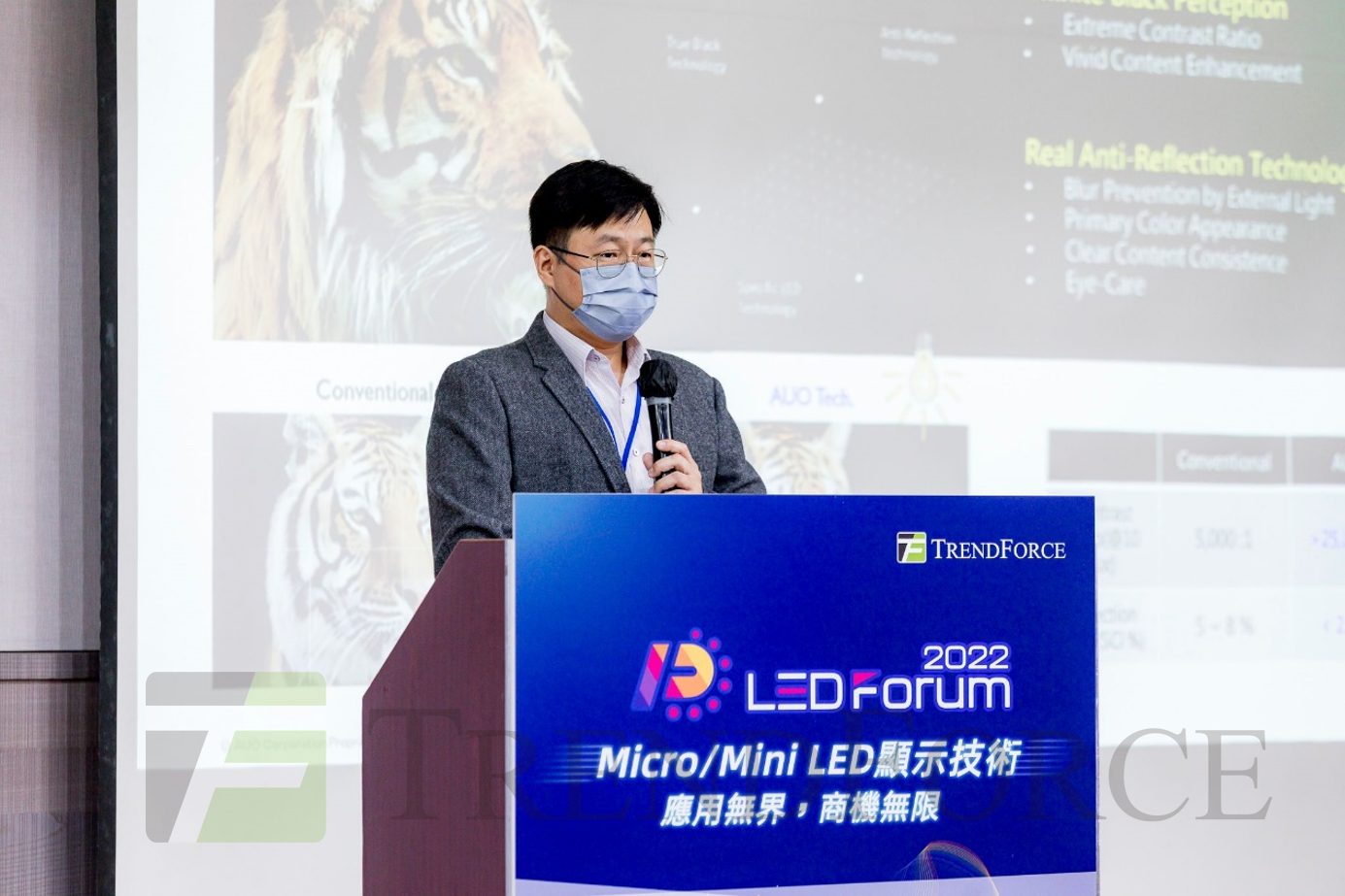
Special Assistant at the Center of New Display Development / AUO
AUO speaker Doctor Hsu Ming-chi commented that the collocation of passive glass backplane driver and seamless splicing technology may become the mainstream design for large Micro LED displays primarily owing to how passive glass backplane drivers can offer high resolution, minimize IC cost, and mitigate backplane bending, which are bottlenecks currently encountered by PCB backplanes. In addition, the lateral plated wire technology of glass metallization has yet to be overcome right now. The rapid decrement of cost, after the technology is resolved in the future, will fully exert advantages of active driver backplanes.

Key Production Solutions for Micro LED Displays
Speaker: Tsai Chi-hao
Chief of R&D Division / Contrel
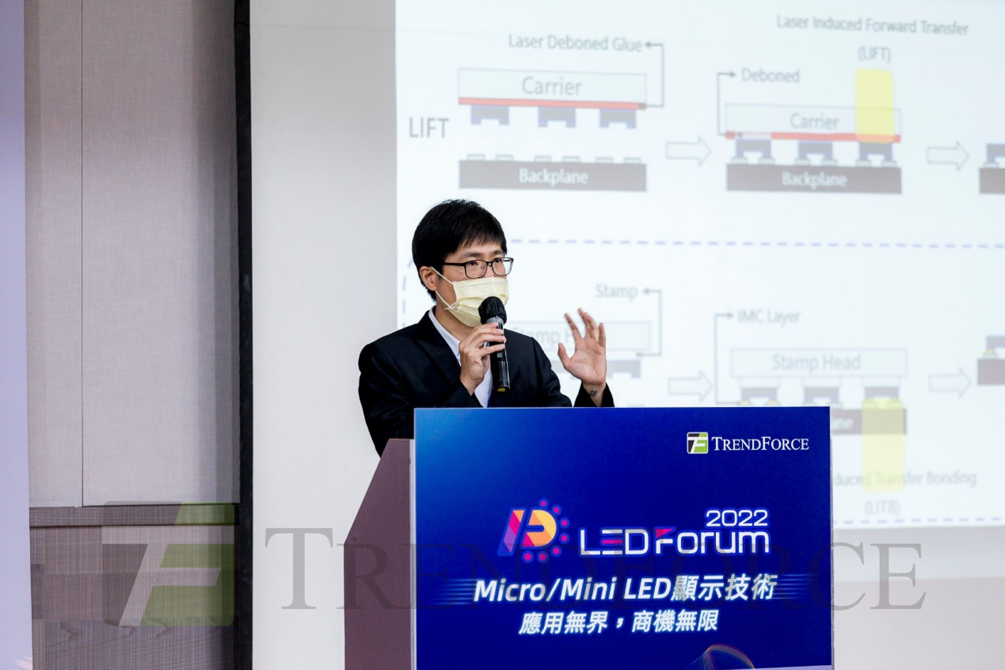
Contrel speaker Tsai Chi-hao commented that Micro LED, after years of development, still has numerous unresolved issues, of which Micro LED mass transfer and selective mass repairing account for the two largest problems since the production cost of the product depends on the speed, yield rate, successful repair rate of mass transfer. As a result, Contrel developed the “laser welding technology” that integrates with stamp transfer, and places a mass amount of Micro LED chips onto the backplane, before welding is done through laser. In terms of the laser source, the backplane would provide the relevant energy for the integration of Micro LED chips and the backplane, which avoids emitting laser source from the Micro LED chips that would damage the consumables and chips.

Applications of Mass Bonding and Mass Repairing Technology in Large Display Market
Speaker: Sean Chen
CEO / Ultra Display
Ultra Display Speaker Sean Chen commented that Micro LED technology, since its initial development, is still left with bottlenecks, such as mass transfer, bonding, repairing, as well as the luminous efficiency of red light chips, and there must be breakthroughs in these bottlenecks before marching towards the mass production phase. Among which, the most crucial bottleneck technology goes to mass transfer, which exhibits different flaws and risks under the development of many suppliers. The development of mass transfer technology, in order to avoid technical issues, must consider the following:
1. Chips: utilization of common LED wafer structure to maximize the flexibility and yield rate of suppliers.
2. Investment: maximize commonalities of equipment, materials, and processes with the existing semiconductor industry, LED industry, and panel industry in order to lower investment risks and elevate probability of success.
3. Production: minimize production procedures and complexity so as to maximize production efficiency and minimize cost.
4. Repair: Future repair issues.

Flexible AM Mini LED Display Technology Innovates, Transcends, and Integrates Future Display Applications
Speaker: Titus Chang
VP / PanelSemi
PanelSemi speaker Titus Chang commented that displays have progressed from CRT to LCD/OLED amidst the shape alterations and performance improvement in flat panel displays, and future displays are gradually transitioning to the more flexible end, which also marks the steady formation of 3rd gen displays. Flexible display technology features rollable function that can be bended inward, outward, and curved, as well as achieves seamless splicing screens. PanelSemi’s AM Mini LED displays are rollable and kept under 1mm in thickness, with no display restrictions through seamless splicing, and are applicable in vast areas such as conference rooms, public infrastructures, advertisement billboards, aircraft cabins, and museums.

Applications of Mini LED Glass Substrates
Speaker: Sun Haiwei
Chief of Development Center / BOE Jingxin Technology
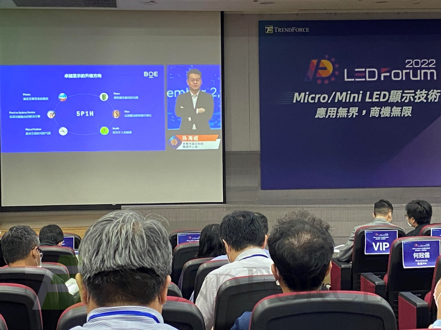
BOE Jingxin Technology speaker Sun Hai-wei attended the seminar through a video call session, and commented that Jingxin Technology is a wholly-owned subsidiary of BOE. The core of BOE’s Mini LED glass substrate is established on three major aspects, which are high-precision glass substrate semiconductor, distinctive AM driver, as well as high-efficiency and high-precision mass transfer technology. The competitiveness of BOE’s Mini LED glass substrate is generated by three areas that are the matured TFT glass technology, no jittering under low gray scale and smooth gray scale transitioning, as well as the exclusive mass transfer technology agreement established with Rohinni. BOE’s full-page design for glass-based Mini LED is most advantageous in creating ultra-thin bodies, where a 65” display would only require one single panel, and a 75” display can be spliced with 2 or 4 panels, while a splicing of 4 panels can attain an 86” AM Mini LED display.

Opportunities and Challenges of Glass-Based Micro LED Display Technology
Speaker: Yao Jiangbo
Micro LED Manager at Innovation Center of Display Technology / TCL
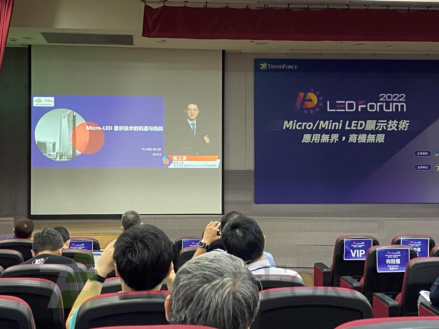
TCL speaker Yao Jiangbo attended the seminar through a video call, and commented on TCL’s comprehensive deployment in applications of various display technology of Micro LED and Mini LED. For direct-lit Micro LED, TCL mainly develops in ultra-large commercial displays, automotive displays, and small wearables, though the company is retained at the product development phase with key technology yet to be resolved. TCL’s current challenges include Micro LED chips, mass transfer technology, backplane technology, driver technology, and assembly technology. Properties including low cost, high reliability, and high current are required for backplanes, and LTPS is the more suitable option for small-sized and high-density products, while Oxide that has a low mass production cost and high performance would become the optimal choice in the future.

(Author: Simon/TrendForce)


 CN
TW
EN

